Hardware Projects
A generic overview about my past, current and (maybe) future hardware related transputer projects.
Other interesting hardware rebuildings are done by Claus Meder, Uwe Mielke, Andre Saischowa and Axel Muhr from Germany.
You can find the documented transputer projects from Axel here: [geekdot.com]
- USB Linkadapter: Full steam ahead!
- KEK Transputerboard 64MB: One 25MHz Transputer on a Eurocard with 64MB RAM.
- IMS B426 Module: A traditionally SIZE 1 TRAM computing module with 4MB RAM.
- IMS B433 Module: A new SIZE 3 TRAM with nine T222 and 64KB RAM for each transputer.
- (TG)²: The Great Transputer Grid, a wall mounted number cruncher.
USB Linkadapter
The bus powered adapter is based on a Cypress USB controller (CY7C68014A-56PVXC) and a Xilinx Spartan II FPGA (XC2S30-5VQG100C). It provides two transputer links at 5, 10 or 20 MHz link speed each with its own subsystem up or down (software selectable). The external link connector is a dual RJ45 connector.
There is a detailed technical note about this adapter:
![]() MB-TCH-003 LINKUSB Hardware description: A device driver writer's guide
MB-TCH-003 LINKUSB Hardware description: A device driver writer's guide
The printed circuit board:
The PCB (100mm x 50.8mm) is a simple four layer FR-4 design with a dedicated ground and separate power plane. Most components are surface mounted and a few passive components are placed on the bottom.
CAM Output: ![]()
RJ45 Jack and Cable:

The link signals use differential line drivers/receivers to provide maximum noise immunity. Because the signal is sent differentially common mode noise is rejected by the receiver up to its common mode rejection limit.
The subsystem (RAE) is implemented with open collector/drain outputs on all three signals and all three values can be read. So there is no preferred direction and the direction depends on the software usage of this signals.
In the standard configuration the green LED shows the link activity and the yellow LED the error status. There brightness is NOT data-sensitive.
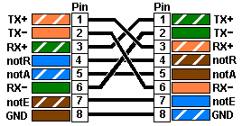
This link connector permits to use standard Ethernet cables. It requires a so called 100baseTX crossover cable which has two pairs crossed and two pairs uncrossed. Depending on the used length CAT5 should be sufficient.
For testing it is possible to use a simple Ethernet loopback cable like the COMPAQ 317463-001. It's also valid to connect both RJ45 jacks with a crossover cable and use the 40MHz link speed to check the cable.
To connect the adapter to a transputer system with Aalener Link connectors (D-Sub with 9 Pins) it can be easily achieved with an customizable Adapter from CUI Inc. (AMK-0001). Only the VCC conductor must be omitted.
Performance:
The unidirectional throughput at 20MHz link speed is the maximum which is possible.
C:\>rspy -l

   # Part  rt Link0 Link1 Link2 Link3

   0 T425C 20 1724K   ...   ...   ...
IMPORTANT: The technique to prevent overlapped acknowledgement occurring on the last byte of the message to avoid the T800C (05 or earlier) output bug isn't possible with this design. But these early types are really rare!
Software support:
For Microsoft Windows (Windows 2000 or later) there is an self-signed device driver available. The device settings can be easily modified in the Device Manager. Instead using the driver directly it's the best to use the LINKIO compatible loadable module (e.g. linkusb.dll). Such a module exists also for Linux/Ubuntu (linkusb.so) and is based on the libusb library.
The "Hello World" Benchmark:
This IMS D7214C benchmark shows the execution time for a full compilation cycle of the hello world classic C-sample.
The following table shows the overall execution time in seconds of the individual statement except the last line which is taken from the ispy output.
| B004PDD | B008MS | USB | Speedup | |
|---|---|---|---|---|
icc hello /ta /si |
2.448 | 2.265 | 1.453 | 1.62 |
ilink hello.tco /f startup.lnk /ta /si |
11.992 | 11.968 | 9.562 | 1.25 |
icollect hello.lku /t /si |
2.738 | 2.796 | 1.968 | 1.41 |
%iserver% /sr /ss /sc hello.btl /si |
0.617 | 0.593 | 0.437 | 1.38 |
ispy.exe |
291 KB/s | 300 KB/s | 1772 KB/s | 6.00 |
The times have dropped significantly on the Kria Transputer Machine. The first two data columns are from two additional transputer modules connected to the Kria via the LinkUSB interface.
| USB-IMSB428 | USB-ZTEX2.04 | KV260 AXI-Light | Speedup | |
|---|---|---|---|---|
icc hello -t9 -si |
0.840 | 0.255 | 0.099 | 8.5 |
ilink hello.tco -f startup.lnk -t9 -si |
6.367 | 1.983 | 0.724 | 8.8 |
icollect hello.lku -t -si |
1.095 | 0.368 | 0.138 | 7.9 |
$ISERVER -sr -ss -sc hello.btl -si |
0.049 | 0.034 | 0.016 | 3.1 |
rspy.exe -l |
T801B 25MHz, 1724KB/s | T805G 66MHz, 24MB/s | T805G 230MHz, 48MB/s | 9.2, 28 |
Please note: The whole compile/link/collect/run cycle is below one second for the transputer hosted programs!
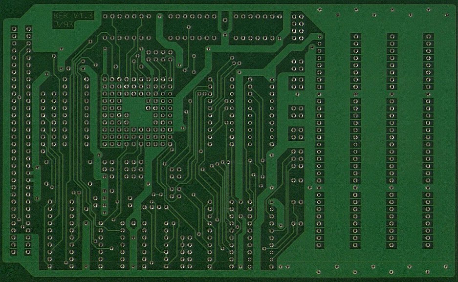
KEK Transputerboard 64MB
In October 2006 I bought a private transputer project and many worthwhile books from Volker B. (Germany). The design was a Eurocard (100mm x 160mm) with one transputer (T805@25MHz), some simple TTL chips and four 30 pin SIMM sockets.
Schematic diagram: ![]()
Four boards were assembled and five were blank. During my searching for more SIMMs I found someone in the United States, who sold 60ns 16MB SIMMs. In short, I bought 36 16MB SIMMs, some TTL's, 19" front covers 6TE, sockets and so on. There was a required modification from the original design, to change the RAS-only refresh to a CAS-before-RAS refresh (with only two scratches, two short wires and a 74F32N replaced by a 74F08N!). I've ordered 3 new boards from pcb-pool and finally I have eight full populated boards with a total of 512MB.
Using 150 ispy 3.23 | mtest 3.22

   # Part rate Link# [  Link0  Link1  Link2  Link3 ] RAM,cycle

   0 T805d-25 338k 3 [    1:0    2:1    3:2   HOST ] 4K,1 65536K,3;

   1 T805g-25 1.8M 0 [    0:0    4:1    5:2    ... ] 4K,1 65536K,3;

   2 T805g-25 1.8M 1 [    4:0    0:1    6:2    ... ] 4K,1 65536K,3;

   3 T805g-25 1.8M 2 [    5:0    6:1    0:2    ... ] 4K,1 65536K,3;

   4 T805g-25 1.8M 1 [    2:0    1:1    7:2    ... ] 4K,1 65536K,3;

   5 T805g-25 1.8M 2 [    3:0    7:1    1:2    ... ] 4K,1 65536K,3;

   6 T805d-25 1.8M 2 [    7:0    3:1    2:2    ... ] 4K,1 65536K,3;

   7 T805d-25 1.8M 2 [    6:0    5:1    4:2    ... ] 4K,1 65536K,3;
The only missing thing is configurable backplane for the 19" 3HE rack.
IMS B426 Module
In my drawer there are a lot of T800D-G25S + HM514400CZ6 and waiting for a SIZE 1 TRAM board.
Not really started. But a lot of thoughts and scribble.
IMS B433 Module
In my drawer there are a lot of T222C-G20S. I'm planning to design a SIZE 3 TRAM with nine T222 each with 64KB RAM. This requires a PGA-Socket which is surface mountable and thin 32kx8 SRAM's for the bottom side.
Why SIZE 3? A 3x3 transputer grid has 12 unconnected links and a SIZE 3 TRAM has 12 external connections for links.
Not really started. But a lot of thoughts and scribble.
(TG)² ... The Great Transputer Grid
It's the place where all of my IMS B426 and IMS B433 will be running...