|
|
| Dual-In-Line Transputer Modules (TRAMs) _____________________________________________________________________ |
| INMOS Limited 72-TCH-029-00 |
In the early days of the transputer, INMOS built a number of transputer evaluation boards. Most are the same size (220mm x 233.4mm), have different transputer configurations, different amounts of memory, transputer graphics or several transputers.
INMOS has also produced boards to fit some particular computers.
The need
It would have been nice if we had been able to offer all the different transputer configurations to fit into these and other personal computers. But instead of about ten different designs of boards, this would have meant 30 different designs. And there was market demand for transputers to plug into VME, to VAX, to SUN, to other workstations, process control computers, minicomputers, mainframes. And there was further demand for more configurations, such as more memory per transputer, more transputers with less memory, or the same memory in much less space, graphics and other different peripherals
Clearly to produce all these different transputer configurations, to plug into all these different computers, would need over 100 different board designs. Even if INMOS could design those, it would be foolish to stock and sell so many different designs. But a genuine market demand existed to be met. Somehow we had to separate the transputer configuration from the computer and its size and shape of board.
Meeting the need
A small range of transputer modules (TRAMS), implemented as modular subsystems, and a small range of motherboards with sockets for the TRAMs, offered this separation.
Users can mix and match different physical sizes of TRAMS - TRAMS with different memory sizes and with different functions. By mixing and matching, many more than 100 different combinations are possible.
An advantage to many customers who have the expertise in interfacing to their own computers is that they can design their own motherboards, and use the ready-built transputer configuration supplied as TRAMs. This greatly reduces the time needed to prototype a transputer system. Many customers are also finding it easier to continue to build their systems based on TRAMS.
The building block
In effect the TRAM is a board level transputer, with a very simple standardized interface. The building block concept is practically realized by integrating memory and peripheral functions on board, and by limiting the pin out to 16 pins (although some modules use several sets of these 16 pins). It is just as easy to build transputer circuits with modules as it used to be to build logic circuits out of TTL.
Several of the TRAMS are densely packed, offering thousands of MIPs, hundreds of MFLOPs and many megabytes, all on a few motherboards in a small box.
Why so small?
The size comes from considering how small a transputer could become. As the chip is about 1cm square, it would not fit with a 0.3” 16 pin DIP, but it would fit into a 0.6” 16 pin DIP Put four of these on a regular prototyping board with rows of sockets on 0.3” centres and you have a set of pins 9-16 just 3.3” away from pins 1-8. Add enough at each end for mechanical fixing and width for a PGA to give the final size.
So the size was primarily chosen to fit standard prototyping boards. Conveniently, the size also fits the IBM PC, VME boards, as well as a host of other computers.
TRAMs are small subassemblies of transputers (or other components with INMOS links), a few discrete components, and sometimes some RAM and/or application specific circuitry. They:
The basic size of a TRAM is 1.05” by 3.66” overall, about half the size of a credit card. This basic size is referred to as Size1. Larger TRAMs can be up to 8.75” by 3.66”, which fits comfortably on an IBM PC board or on a VME board (this largest size is referred to as Size8). Smaller TRAMs (hybrids or silicon, not yet implemented) can be as small as a 16 pin DIP with leads on 0.6” centres.
The standard pinout and standard sizes of TRAMs make it very simple for users to build customized motherboards with sockets for TRAMs. These can either be in prototype form (Perfboard, Vectorboard or Veroboard), or in printed circuit form.
TRAMs may be plugged into the TRAM sockets on any of a wide range of TRAM motherboards made by INMOS and many of INMOS’ customers, to fit most of the popular computers and busses.
Most of the motherboards include C004 link switches, so that users can configure their own networks to match the structure of the problem they are trying to solve.
The TRAM standards referred to above are independent of:
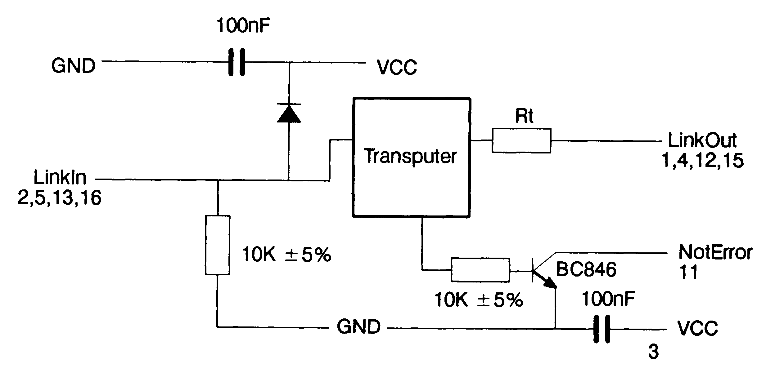
The pins include four INMOS links, which require no off-module buffering.
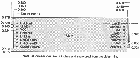
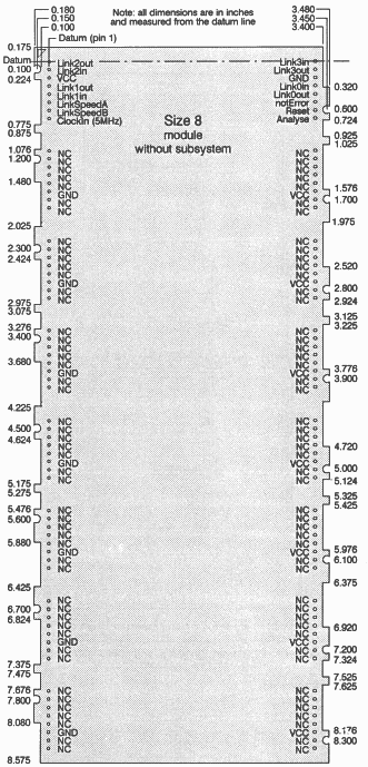
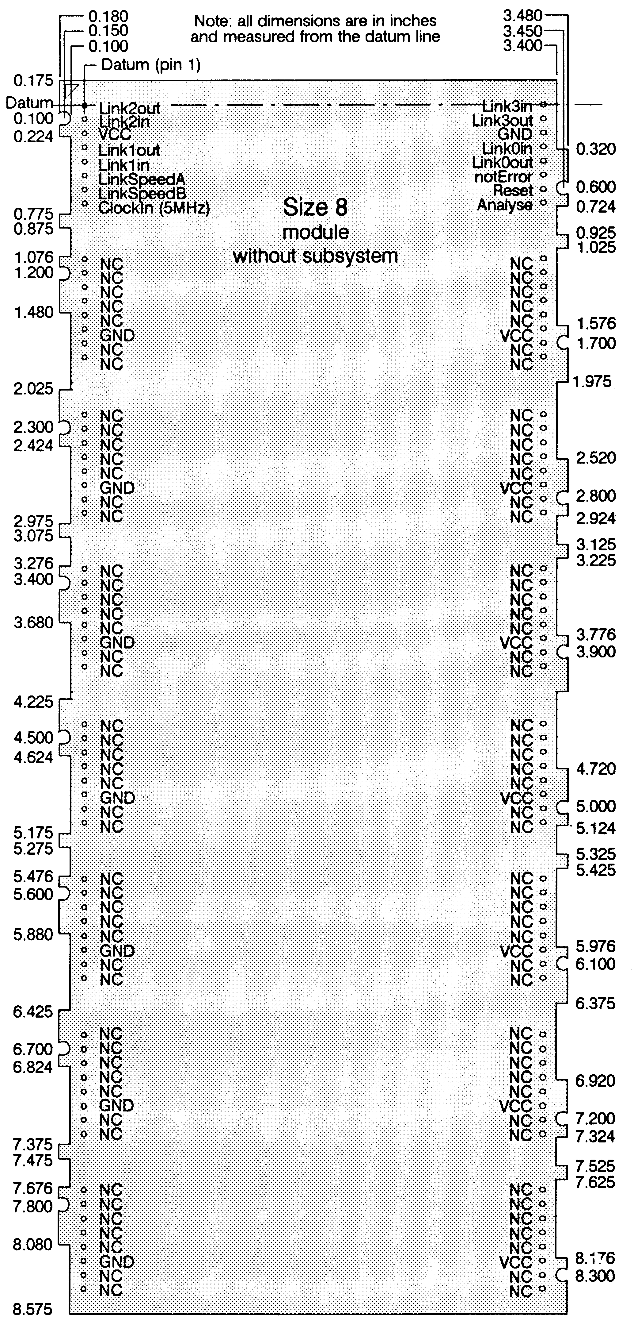
Table 1 shows the pinout. This pinout has been chosen partly to simplify layout of the motherboard, and partly to simplify the layout of the TRAM.
|
When LinkSpeedA and LinkSpeedB are both low, the TRAM links operate at 10Mbits/s. When they are both high, the links operate at 20Mbits/s. Other states of these pins are reserved for future enhancements.
The notError signal is driven by an open collector transistor so the signal can be wire ORred. This allows for the error line to be bussed in the same way as Clock, Reset, and Analyse. The fan-in of the notError signal must be controlled, and it is recommended that no more than ten notError outputs are wired together.
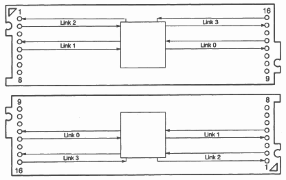
Pin 1 is marked by a silk screened triangle.
Figure 1 shows two adjacent Size1 TRAMs side by side. Notice that the orientation of the two modules is different. This difference in orientation serves two purposes: cooling of Size1 modules is improved; and it makes it possible at some future date to have Single-In-Line modules.
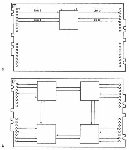
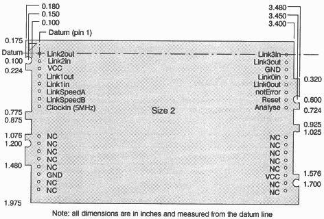
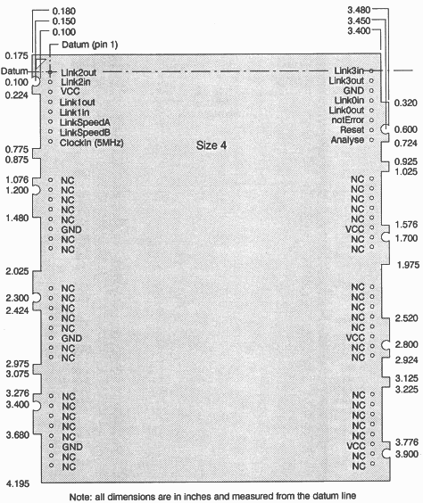
Many modules, and all the early products IMS B401 to B405, contain a single transputer, and so do not need more than one set of 16 pins for electrical signals. Modules larger than Size1, however, are assembled with extra sets of 16 pins; the extra pins give mechanical support, allow modules to be stacked, and provide extra GND and VCC pins. A Size2 module with one transputer is shown In figure 2a.
TRAMs maybe built with more than one transputer, or with transputers having more than four links. An example of a possible TRAM with more than one transputer is shown in figure 2b. This has four transputers connected as a square, in the same way as the IMS B003 and B006. (In practice, if INMOS were to produce a TRAM with four transputers, the links would probably be routed to make better use of standard motherboard connections.)
The detailed pinouts of larger modules are shown with the mechanical details in section 8 and assume that each TRAM has a single transputer, with four links.
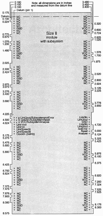
Notice that the Size2 module and the Size4 module have the pins which are actually used at one end. The Size8 module (when it has a subsystem capability) has the pins which are used in the middle.
Standards for pinout of transputers with more than one transputer are to be defined.
TRAMs may include application specific circuitry which requires pins other than the standard 16 pins. Examples are peripheral controllers or pipelines used for graphics or signal processing. The recommended connector for these is a strip of pins on 0.1” grid, such as a stripcable socket will attach to.
It is useful for TRAMs to be able to control a network of transputers and/or more TRAMs. Such a slave network is known as a subsystem of the master, and the set of control signals from the module are described as a subsystem port.
The subsystem port consists of three signals: SubsytemReset and SubsystemAnalyse, which enable the master to reset and analyse its subsystem; and SubsystemnotError, which is used to monitor the state of the error flag in the subsystem. The polarity of these signals is such that a motherboard can be built with a master TRAM controlling slave TRAMs via its subsystem port with no buffering or gating. (Note that a change of polarity may be required for a subsystem port which goes off the motherboard.)
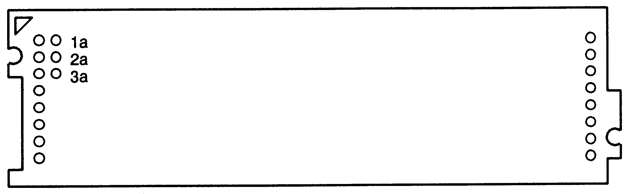
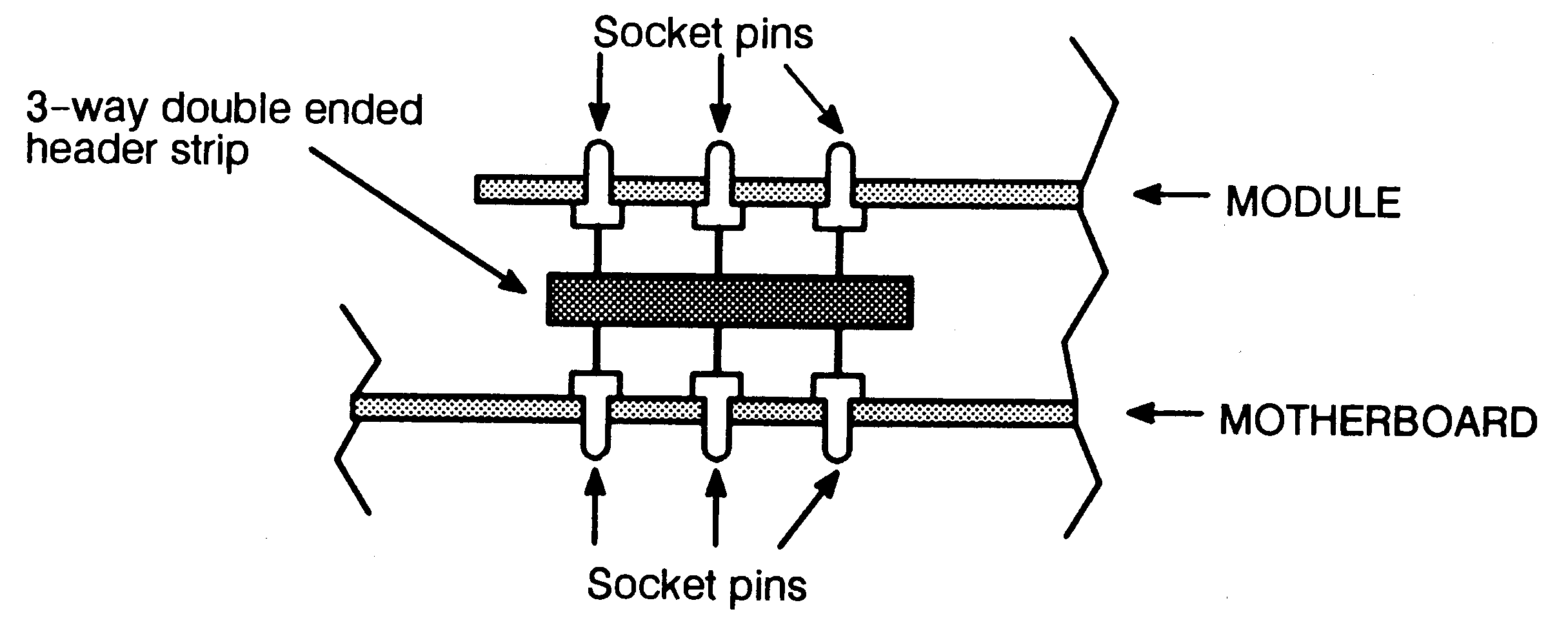
The three subsystem signals are located on low profile sockets which are positioned 0.1” inside the standard module pins 1-3. This is illustrated by figure 3.
The pinout is as follows:
| Pin | Signal |
| 1a | SubsystemnotError |
| 2a | SubsystemReset |
| 3a | SubsystemAnalyse |
The sockets are fitted into the module PCB upside-down. The motherboard into which the module is plugged will also have three such sockets In the corresponding positions, but fitted from the component side in the usual fashion. The connection between the module and the motherboard is then made by a double-ended header, strip (see figure 4). This arrangement ensures that if the subsystem port of a module is not used, the module remains mechanically compatible with modules which do not have subsystem ports.
Subsystem registers
The subsystem is controlled by reading and writing to addresses in positive address space (i.e. location zero onwards). On all INMOS evaluation boards and TRAMs, two BYTE locations are used, where each byte is the least significant byte of a 32 bit word. A further two locations control parity generation logic, which will be described in section 3.6. These four locations are permitted to repeat throughout the whole of the positive address space.
The subsystem registers are located at the following addresses for 32 bit transputers
| Register | Hardware byte address |
| SubSystemResetLatch (write only) | 00000000 |
| SubSystemAnalyseLatch (write only) | 00000004 |
| SubSystemnotError (read only) | 00000000 |
The subsystem port operates as follows:
Writing a 1 into bit 0 of #80000000 asserts SUBSYSTEM Reset;
Writing a 0 into bit 0 of #80000000 deasserts SUBSYSTEM Reset. Writing a 1 into bit 0 of #80000004 asserts SUBSYSTEM Analyse; Writing a 0 into bit 0 of #80000004 deasserts SUBSYSTEM Analyse. A 1 read from bit 0 of #80000000 indicates that SUBSYSTEM Error is TRUE. A 0 read from bit 0 of #80000000 indicates that SUBSYSTEM Error is FALSE. |
The subsystem is reset or analysed under the control of the transputer on the TRAM, but must also be reset when the TRAM itself is reset. To pass the signals on to the subsystem, the following combinational logic is included:
SubsystemReset = Reset OR SubsystemResetLatch
SubsystemAnalyse = Analyse OR SubsystemAnalyseLatch |
The latches are initialized at power-on to be inactive.
Note that SubsystemError does NOT propagate to the TRAM’s notError pin.
Multiple subsystems
TRAMs may contain more than one subsystem port. They should have their locations separated by 16 bytes.
TRAMs may include parity logic for external RAM. The implementation on TRAMs must ensure that there is no way that corrupt data can reach any other transputer.
One way to achieve this is that if a parity error occurs, the wait signal is held active so the memory cycle does not complete. All data in memory is lost, however, when an error occurs, and the memory cycle is slowed down by the parity check.
Parity checking may be enabled or disabled by writing to a parity control register. If parity is enabled and an error occurs, the error is ORed in to the notError signal from the module. Information on the cause of the error can be found by examining the parity status register.
Reset disables parity checking and deasserts MemWait. When the transputer is analysed, MemWait is deasserted and the contents of the parity status register are preserved.
The parity registers are as follows:
| Register | Hardware byte address |
| Parity control (write only) | 00000008 |
| Parity status (read only) | 00000008 |
The locations are used as described below:
Writing a 1 Into bit 0 of 80000008 enables parity error detection;
Writing a 0 into bit 0 of 80000008 disables parity.
Reading the contents 80000008 returns the status of the parity detection hardware.
| Bit | Status |
| Bit 0 | Indicates a parity error has occurred. |
| Bits 1,2 | Indicate the BYTE in which the error occurred. (Bit1 is lsb). |
| Bits 3..n | Indicate the BANK in which the error occurred. (Bit3 is lsb). |
The memory map should be of the form:
| ROM | top of memory |
| Peripherals | |
| Subsystems | |
| External RAM | |
| On-chip RAM | bottom of memory |
In the particular case of TRAMs with 32 bit transputers, the memory map should be as follows:
| Byte address | Description | Comment |
| 7FFF FFFF | Bootstrap program requires | |
| 7FFF FFFE | Boot from ROM | ROM at top of memory. |
| Peripherals | If used | |
| 0000 000C | These locations must | |
| 0000 0008 | Parity status and control | be decoded as a set |
| 0000 0004 | SubsystemAnalyseLatch | of four, even if Parity |
| 0000 0000 | SubsystemResetLatch | is not used. |
| 8FFF FFFF | RAM | Both internal and |
| Memstart | RAM | external RAM |
Byte address 7FFF FFFE will contain a backward jump to the bootstrap.
Substantial logic can often be saved by not fully decoding the hardware address. An effect of not fully de. coding the address is that hardware can appear at multiple addresses.
In particular, if the module does not have a subsystem, the RAM can repeat throughout the address space, including the positive address space (above location 0).
The Subsystem and parity locations can also repeat throughout the positive address space.
Link outputs must be terminated so that the combined output impedance of the transputer plus termination resistors is 100 ohms ±20%. For the optimum value of resistor, see the appropriate transputer data sheet.
Link inputs may be taken off a module motherboard and so must be protected from positive ESD by a diode to VCC. Signal diodes such as 1 N4148 or LL4148 may be used. To prevent an unconnected link input from floating high, link inputs must be pulled down to GND by a resistor, preferred value 10K ± 5%.
The notError output is a wired OR signal driven by an open collector or an open drain. Maximum leakage should not exceed 10 microamps. Maximum saturation voltage when the transistor is ON and is sinking 10 mA should not exceed 0.4 V. A suitable transistor is BC846 (SOT23) with a 10K resistor between the transputer’s Error pin and the transistor base. The pullup resistor on the module motherboard should draw between 5mA and 10mA when a transistor is ON.
Although the above is conservative and should allow a fan-in of several hundred, it is recommended that the fan-in is limited to 10.
These signals are connected directly from the TRAM pins to the transputer. They must always be driven by buffers on the module motherboard. Because the motherboard will often have filters on the Reset and Analyse signals, the Reset pulse width should be much wider than specified for the transputer. Recommended pulse width is 5 ms, with a delay of 5 ms before sending anything down a link.
The TRAM must not present excessive capacitance to the clock input signal. The clock input should therefore be limited to a single load, which should be connected to the TRAM pin by a trace no longer than 30mm.
Particular care should be taken on the module motherboard to ensure that the clock input is clean, with fast edges, minimal undershoot, and minimal jitter (see transputer data sheet for clock specification).
The notError input should not have a pullup resistor on the TRAM. The pullup resistor must be on the motherboard.
Adequate high frequency decoupling capacitors must be used. In particular there should be decoupling capacitors close to the GND pin and to the VCC pin of each TRAM. Recommended value is 100 nF, preferably at least half as many as the module has ICs.
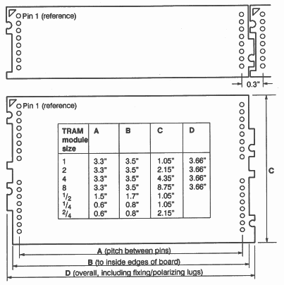
In the following, dimensions are quoted in inches for PCB length, width and related dimensions; all other dimensions are quoted in millimetres.
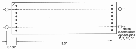
The basic size of a TRAM is a very wide 16 pin DIP, with 3.3” between the two rows of pins. These TRAMs fit on a 3.6” pitch on their length, and a 1.1” pitch on their width. Extra length is added beyond the pins to hold the pins, to provide for mechanical fixing, and to polarise the module shape.
TRAMs can be made larger than the standard size by keeping the 3.3” between pins and using two or more sets of the 16 pins.
TRAMs can be made smaller than the standard size, down to a 16 pin DIP with 0.6” between the two rows of pins, or 1.5” between the pins. These sizes will normally be used for single chip modules or hybrids.
In general the printed circuit TRAMs are longer than the pitch between the two rows of pins. The TRAMs are also wider than the 0.8” suggested by 16 pins. The small TRAMs may be side-brazed DIPs, as short as 0.8” long. The top drawing in figure 6 shows a Size1 module and how the jigsaw pattern fits together between adjacent modules. The lower drawing in figure 6 shows the various sizes of TRAM. Detailed dimensions of the different sizes are given in section 8.
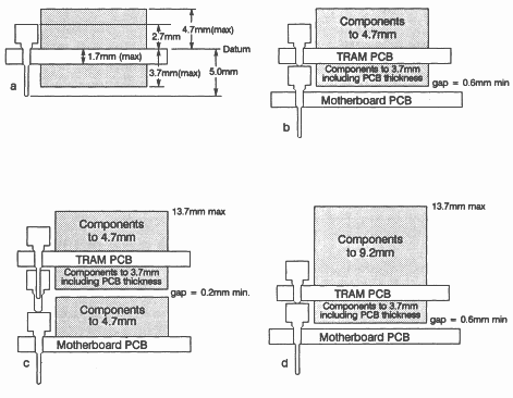
There are no vertical height constraints for TRAMs. However, keeping the height of a TRAM, both below and above the board, within certain limits allows the TRAM to fit together with other TRAMs and motherboards.
Figure 7a shows height specifications, both above and below the TRAM PCB. Figure 7b shows how this vertical size fits onto a motherboard which has no components under the TRAM. Figure 7c shows the same TRAM fitted above components on a motherboard, using spacer socket strips to gain extra height.
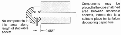
Figure 7d shows another height specification which allows components such as zip packaged ICs and SMB connectors to be used on the TRAM, whilst permitting these TRAMs to fit onto motherboards in a 0.8” pitch card cage. Note that this is only possible when there are no components under the TRAM on the motherboard.
The TRAMs are specified to make it possible to stack one TRAM above another in some circumstances. The combination of physical and thermal constraints on stacking has meant, however, that for a number of TRAM implementations stacking is not possible. The figure showing stacked TRAMs (which appeared in earlier versions of this document) has therefore been removed in this version.
It is recommended that any component reaching a maximum specified height has an insulating surface.
Note that the datum for component heights on both sides of the TRAM is the component side surface. This datum is also used for the stackable socket to minimize tolerance buildup.
Components must not interfere with the TRAM pins, and so the area shown in figure 8 must be left free of components.
TRAMs should be designed so that cooling air can flow freely across the width of the the module, or in other words parallel to pins 1 to 8 rather than from pin 1 to pin 16. Care should also be taken to ensure that the surface of a module is not too flat: projections cause turbulence which improves cooling.
The stackable pin socket is shown in figure 9.
Approved manufacturers of the stackable socket pin are (with part numbers): 1
| individual socket pin | Strip of 8 sockets | |
| Scott | 128-446 | 15108-128-446 |
The individual socket is used on the TRAMs themselves. Strips of 8 sockets are used on TRAM motherboards and as spacers (as in figure 8) between TRAMs and motherboards.
The component height given in figure 7 means that there is not enough height for conventional sockets for the components. A number of manufacturers make sockets which fit into a PCB in such a way that the thickness of the PCB Is used for the socket, rather than extra height above the board.
INMOS has seen and used the following sockets. No particular recommendation for any of these is given or implied. Other manufacturers have shown data sheets for similar sockets with a height of approximately 0.8mm. The Augat ’Holtite’ sockets, which sit below the PCB surface, have been seen but not used. The
Augat ’Soldertite’ sockets have similar dimensions to the Harwin 3153 and have been seen in prototype quantities. All of the sockets are available individually or assembled into strips; some are available in DIP and PGA format.
| height | ||
| Manufacturer | type | above PCB |
| Harwin (UK) | H 3153-01 | 0.38mm |
| Mark Eyelet (AMP) (US) | M8043PEC | 0.2mm approx |
| PreciDIP (Switzerland) | 014-92-001-41-012 | 0.4mm |
| Advanced Interconnections (US) | type -85 | 0.78mm |
| Harwin (UK) | H 3155-01 | 1.2mm |
| PreciDIP (Switzerland) | type 1407 | 0.8mm |
The preferred socket to fit on the solder side of the TRAM is Harwin H 3153-01, and on the motherboard also. Samtec pin strip HLT-03-G-R is suitable for connecting between these sockets.
The TRAM pins/stackable sockets will plug into any standard IC socket. To meet the component heights given in figure 7, the stackable socket (see section 6.1) must also be used on the motherboard.
Motherboard sockets for the Subsystem signals should be the 0.38mm or 0.4mm sockets referred to above.
Vibration tests have shown that in a normal office or laboratory environment, the TRAMs remain plugged into their sockets. In transit, however, or in an environment where there is vibration, some form of mechanical retention may be necessary.
The detail drawings of the module sizes in section 8 show fixing holes in the modules. Similar fixing holes should be drilled in the motherboard as shown in figure 10. M2.5 nylon bolts maybe used between these fixing holes to secure the modules.