|
|
| IMS B006 A single board computer using 9 IMS T212 transputers _____________________________________________________________________ |
| Abhay Vadher February 1987 |
December 2, 1986
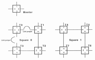
This technical note describes the IMS B006 evaluation board. The B006 board enables the user to evaluate multiple transputers. It is a double extended eurocard containing nine T212 transputers when fully populated, one of the T212’s is referred to as the master transputer and the rest as modules (numbered T0 ... T7).
The T212 transputer is a 16 bit programmable VLSI device, made up of a single level microcoded processor, four serial point to point communication links, 2Kbytes of fast static ram and an external memory interface.
The external requirements for the master transputer are 7Kbytes of EPROM, 1Kbyte of peripheral address space, 54Kbytes of RAM and an RS232 interface.
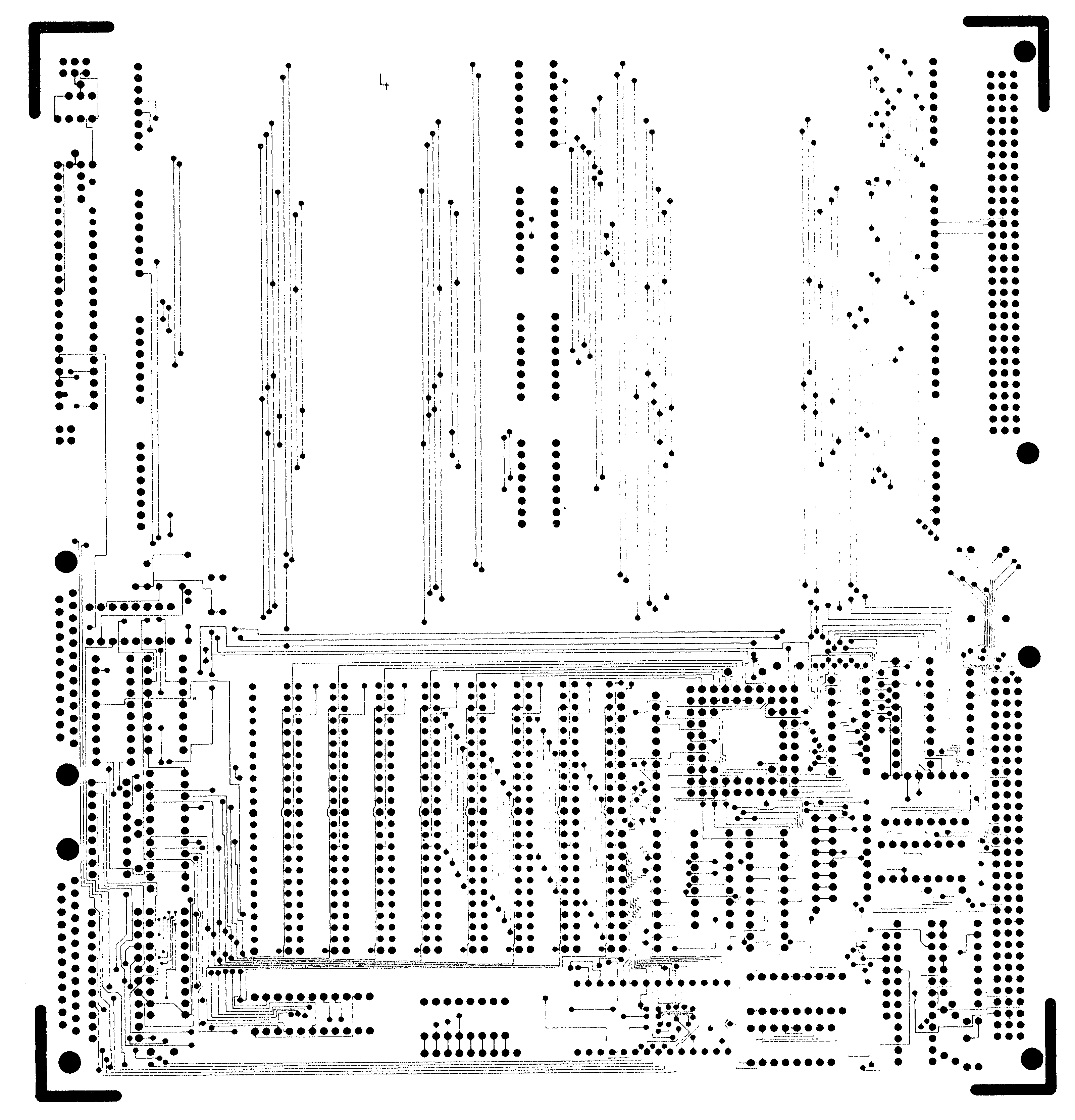
The eight modules are configured in two squares with two links from each transputer brought to the edge connector as shown in figure 1. However one module (T0) can be fully isolated since all the links from module T0 are brought to the top and bottom edge connectors and the square is completed via the use of link jumpers (many other configurations are also possible).
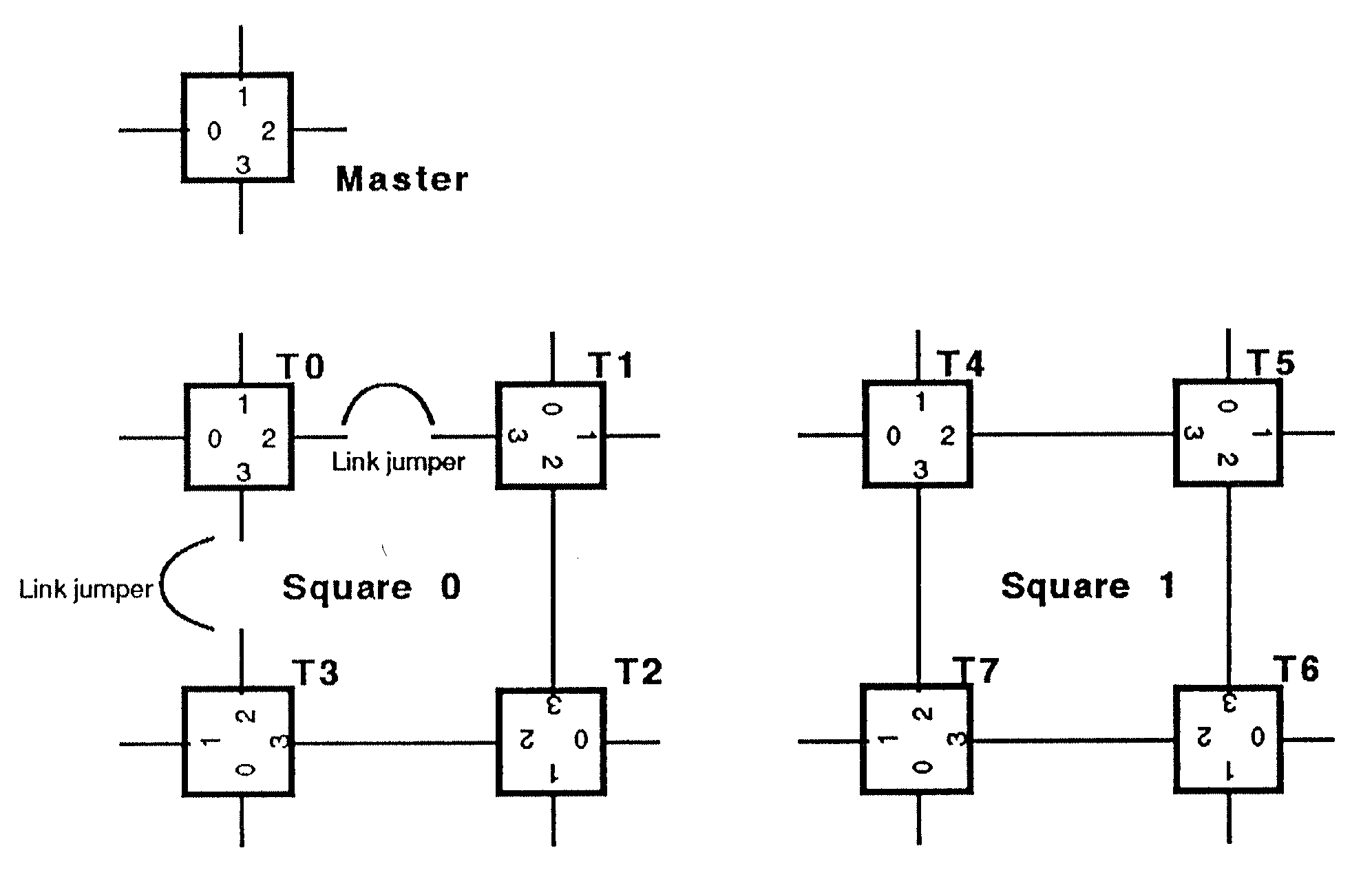
The interface from the B006 is via two 96 way DIN 41612 edge connectors, as shown in figure 2. The bottom edge connector is a simple superset of edge connectors used by other INMOS evaluation boards. The top edge connector is specially made to cater for 32 INMOS link cable sockets.
The eight modules as shown before are connected in two squares, with links 2 and 3 of each transputer connecting them in squares.
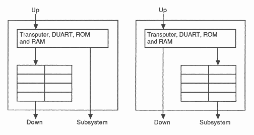
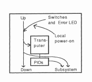
The eight transputer modules are reset or analysed from the down or subsystem of the master transputer which is controlled by a switch on the board as shown in figure 3.
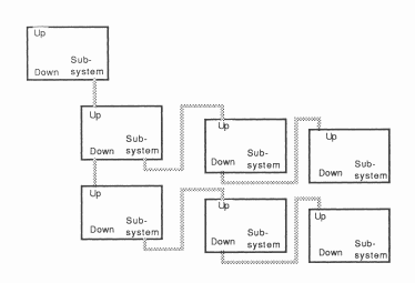
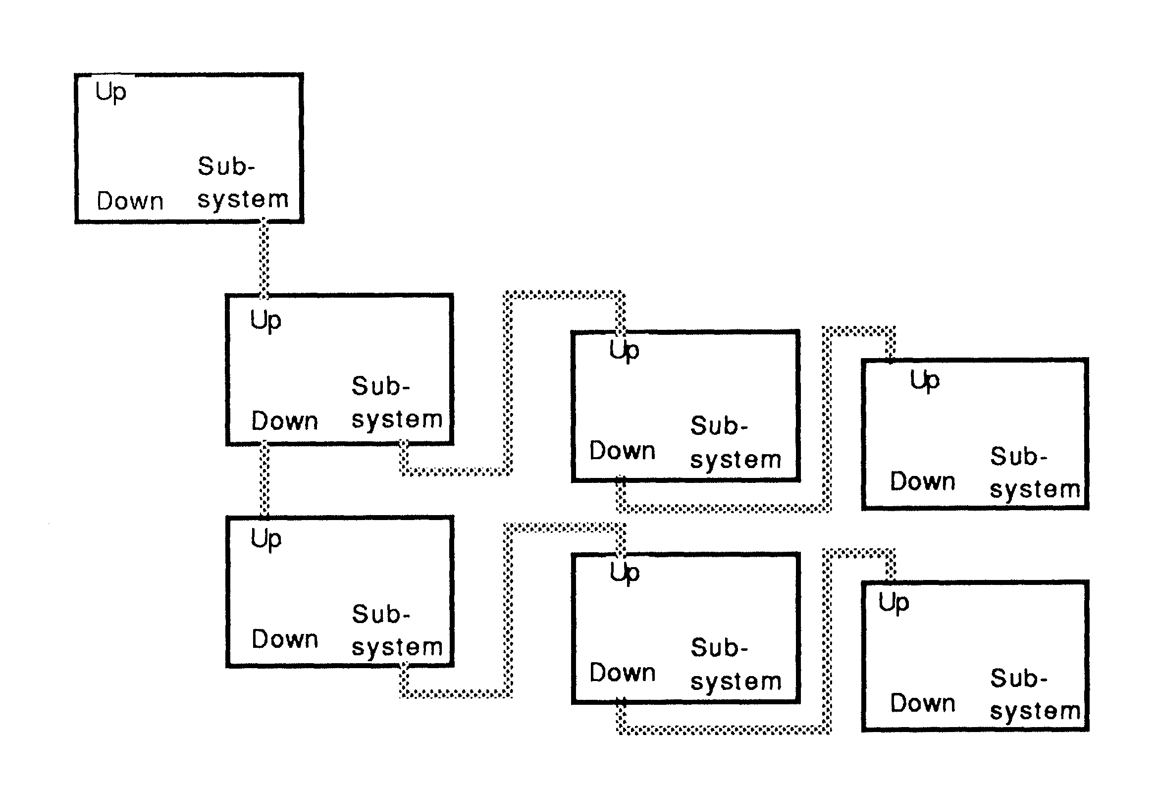
One board can control a subsystem of an arbitrary number of other boards. This is achieved with three sockets on the bottom edge connector, which are referred to as UP, DOWN and SUBSYSTEM. Figure 4 below shows a board at the top with its subsystem socket wired to the up socket of the board below. Subsequent boards are daisy chained by wiring the down socket of one board to the up socket of the board below. Each board in a subsystem can control a further subsystem.
The notReset and notAnalyse signals flow in the direction of the arrows shown in figure 5 and the notError signal flows in the reverse direction from down to up.
The module described here conforms to the INMOS 16 pin module specification. The specification requires the modules to have the standard pinout as shown in figure 6, link protection from electrostatic discharge (ESD) of up to 2KV and the 16 pin module size (3.5’ × 1.05’). The ESD test on the module meets MIL-standard 883B and method 3015.1.
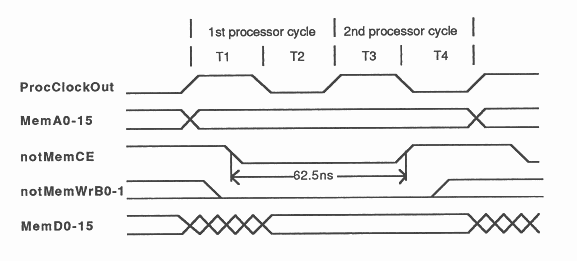
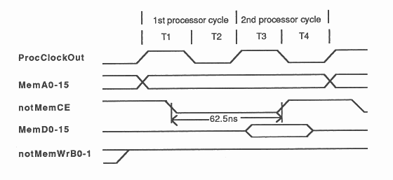
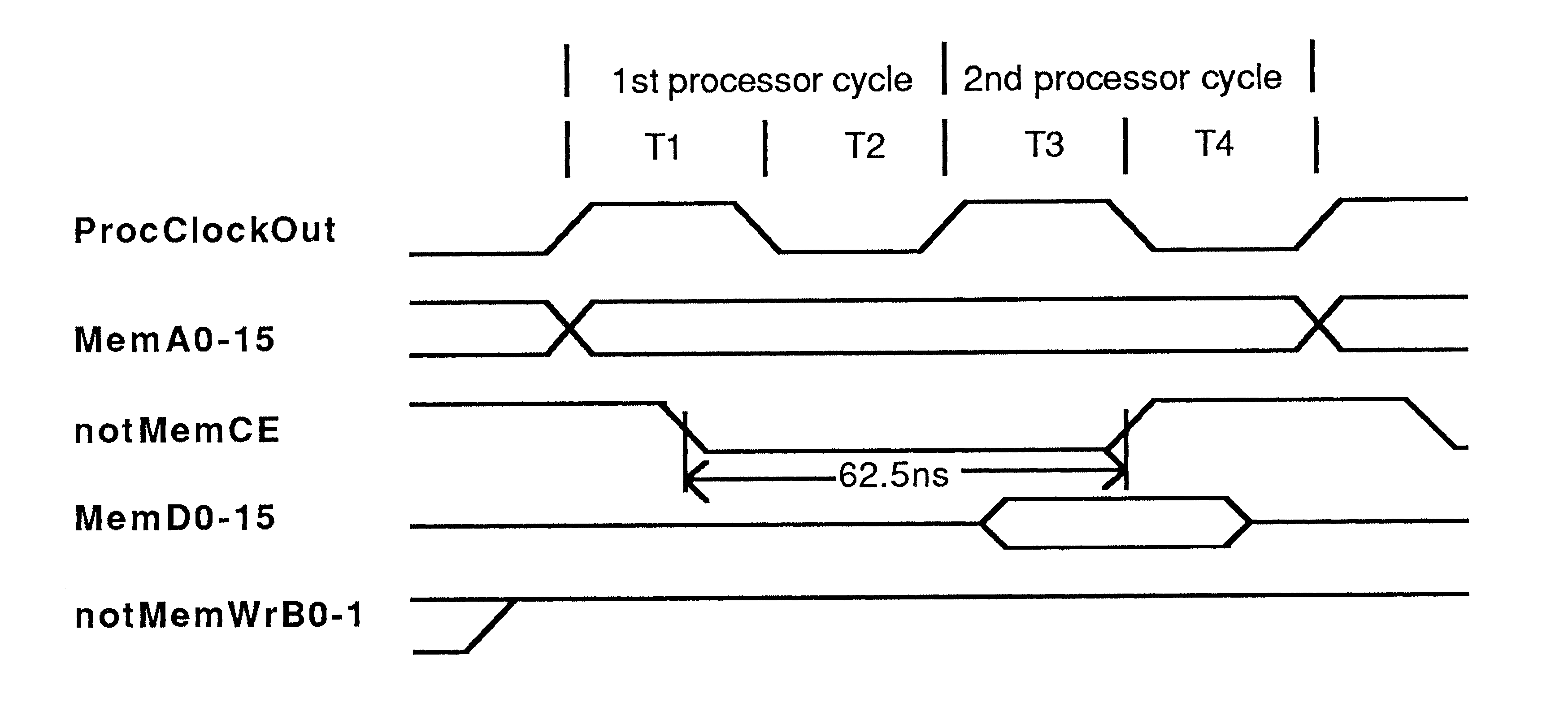
The static ram used on the module has an access time of 25ns. The reason for using such fast static ram was to enable the use of fast transputers (T212-20) working full speed, that is without the use of wait states. The overhead of the chip enable (notMemCE) output delay and the data setup time is half a processor cycle, therefore ram access times of less than 37.5ns are needed. The 25ns ram used will eventually allow the use of T212-22 transputers when available. The timing diagram below shows the margin required to access external memory without wait states.
T212 Word Write cycle:
|
|
T212 Word Read Cycle:
|
|
The use of a single bank of memory assisted in avoiding decoding delays and also helped reduce capacitance on the address lines, which could add to the margin required to access the memory without any wait states.
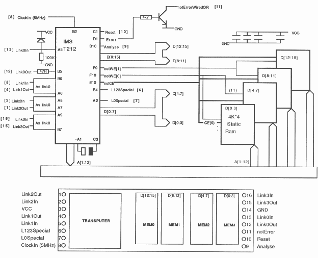
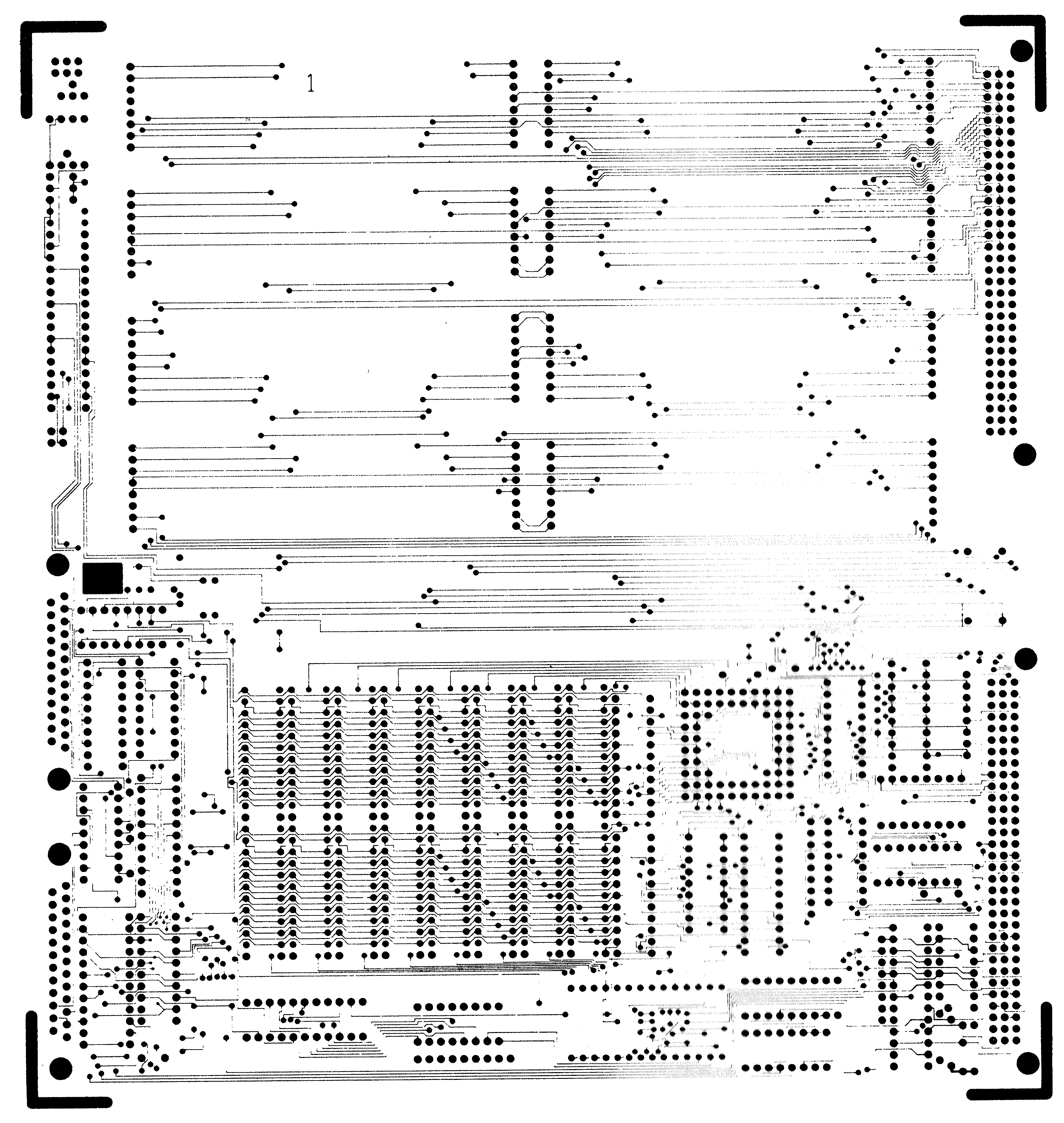
The module consists of a T212-20 and 8Kbytes of fast static RAM. The logic for each complete module is shown in figure 6. The RAM is provided by four 4k×4 static rams. Apart from the RAM and Transputer there are a few discrete components for the links, for error and for decoupling.
The links of all the module transputers are capable of operating at speeds of 10 or 20 Mbits/s. The link speed selection can be performed by two switches provided on the board.
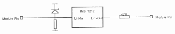
Links 2 and 3 of each module transputer except T0 are connected on the board and have a simple termination on the linkout signals. The termination resistor of 47 ohms, combined with the output impedance of the linkout circuit, gives a termination impedance of approximately 100 ohms.
Links 0 and 1 of all the module transputers, which are brought to the edge connector, also have 47 ohm resistors on the link outputs. The link inputs also need pull down resistors in case a link is not connected. The link inputs are more sensitive to electrostatic discharge (ESD) than the link outputs, and so the link inputs which connect to the edge connector are protected by schottky diodes; with the diodes the transputer can withstand ’zap’ tests of up to 2kV without damage. The link circuit is shown in figure 7.
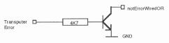
The error output produced by the transputer is active high, which is suitable when there is one transputer on board but causes extra wiring and logic if there are many transputers on a board. To simplify the wiring, a notErrorWiredOR signal is generated by a resistor and transistor, as shown in figure 8.
The power supply decoupling for the RAM and transputer is provided by surface mounted capacitors that are close to the components to provide good decoupling. In addition to the power supply decoupling a further capacitor is needed between CapPlus and CapMinus to decouple an internal power supply used by the phase locked loop/clock multiplier. A 1uF tantalum capacitor is used for this purpose.
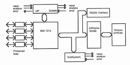
The master transputers is composed of three main elements:
A block diagram of the master transputer is shown in figure 9.
The T212 sixteen bit transputer has 2Kbytes of memory internally and can access a 62Kbyte access space externally. The memory map of the transputer is signed, with the internal memory starting at the most negative address (HEX 8000 to HEX 87FF). The external memory starts at HEX 8800.
The B006 board provides 54Kbytes of external RAM, 7Kbytes of EPROM and 1Kbyte of peripheral access space, which provides the system control signals, to give the user the possibility of connecting and controlling a number of INMOS transputer boards together.
This is a simple synchronous design with the memory decode signal enabling the memory and the noWriteEnable[0:1] strobes, driving their respective arrays to select read/write cycles. The address bus from the transputer is buffered by two F245’s which are permanently enabled.
The external RAM has a simple fast decode, provided by a multiplexor with an access time of 9ns worst case as shown in figure 10. The access time for the external RAM is 45ns and because of the load on the address bus, the address bus is buffered. A combination of these factors means that the external memory interface has the addition of one wait state, when accessing the external RAM.
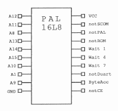
The logic for address decode for the ROM and peripherals were implemented in PAL logic. In the design description, that logic is described in terms of the programming language used by the CUPL (universal compiler for programmable logic) programming system (available from Assisted Technology for personal computers).
The address decoding is performed by a 16L8 PAL as shown in figure 11, with an access time of 15ns worst case.
The address map of the master transputer is shown below:
| 7FFF | Top of EPROM | |
| .... | 7Kbytes | |
| 6400 | Bottom of 7k-bytes of EPROM | |
| 6200 | RS232 data: bit D0 is received data from | |
| D type socket (terminal), | ||
| bit D1 is received data from | ||
| plug (host computer) for autobaud | 1Kbyte | |
| 6101 | Subsystem latch in PAL: D0 read = Error; | peripheral |
| D0 write = Analyse | address | |
| 6100 | Subsystem latch in PAL: D0 write = Reset | space |
| (write a ’1’ to assert Reset) | ||
| 6000 | DUART registers byte mapped (Byteaccess-high) | |
| 5FFF | Top of external RAM | |
| .... | 54Kbytes | |
| 8800 | Bottom of 54k-bytes external RAM with T212 | |
| 87FF | Top of on-chip RAM for T212 | |
| .... | 2Kbytes | |
| 8000 | Bottom of 2k-bytes on-chip RAM | |
The address decode PAL is enabled by the notCE strobe. The PAL performs the functions:
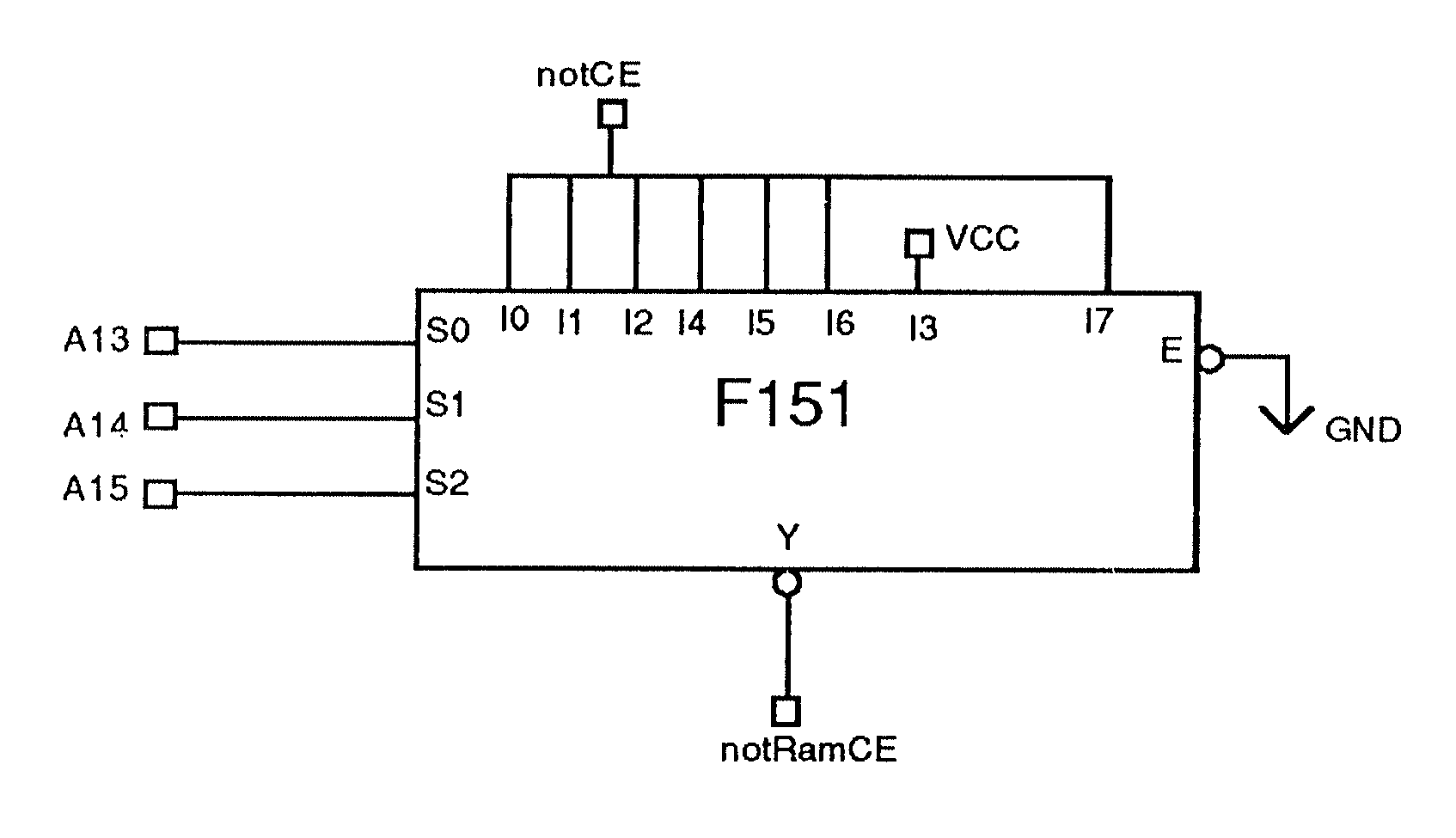
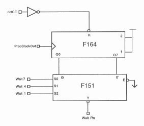
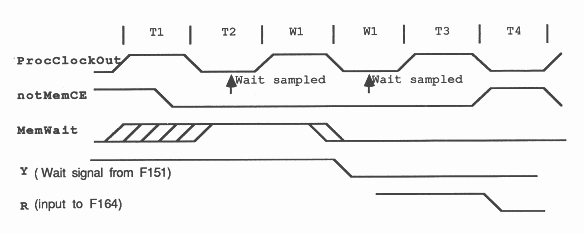
Memory cycles can be extended indefinitely by asserting the wait pin on the transputer high at the correct time. The wait pin signal is sampled during the first processor cycle of the memory access. If it is found to be high, processor cycles are added to the memory access until subsequent sampling detects the wait pin signal to be low, at which time the memory access proceeds normally.
The wait state generator here consists of a simple digital delay line, as shown in figure 12 which is cleared until the notCE strobe becomes asserted and thereafter clocks a high through the register. The output of the shift register that goes to the wait pin of the transputer is selected by a 8×1 multiplexor whose output is determined by three wait selection lines from the decode pal. This provides us with a cycle by cycle programmable wait state generator and thus the devices in the system can operate at their own rate.
Note from the timing diagram:
Single wait timing diagram:
|
|
The EPROM circuit is simple with the notCE strobe and notROM address decoded signal, controlling the data output from the EPROM. The EPROM contains a monitor and self test software.
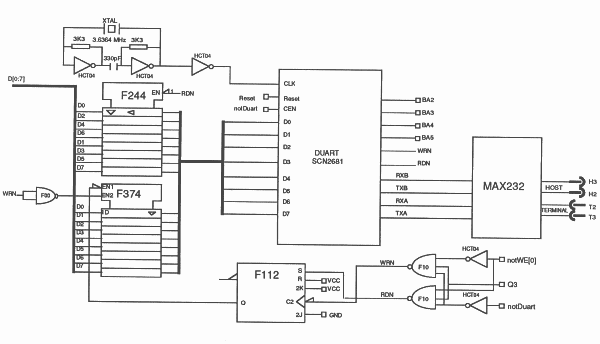
The DUART (SCN2681) enables the master transputer to have an RS232 interface. Figure 13 shows the DUART circuit.
The DUART cannot be directly interfaced to the T212 working at full speed. This is because the T212 turns round the bus within 50ns after notCE becomes deasserted in the last cycle. We must thus buffer the DUART databus and control the buffer with the DUART enable strobe notDuart, generated by the address decode PAL (16L8).
However we can still get bus contention between the buffer (F244) and the DUART if a write cycle occurs immediately after a read cycle. We get around this problem by delaying the start of the cycle as far as the DUART is concerned. This delay together with the delay required for the read (RDN) and write (WRN) strobes, results in a T212 memory cycle with seven wait states.
Another problem is the data hold time required by the DUART (20ns), for this the databus is split into a driver (F244) and a receiver (F374) which latches the data.
The driver is enabled by RDN. The input data buffer (F374) is clocked when data is valid and enabled from when WRN is asserted via a JK-flipflop, until it is disabled by RDN being asserted to avoid bus contention.
The actual RDN and WRN strobes are decoded from the notDuart and notWE[0] with the Q3 output from wait state generator by two NAND gates.
The IMS B006 shows that a high performance multi-processor system can be designed using transputers. The board will allow the user to exploit concurrency and can be programmed in most high level languages. To gain most benefit from the transputer architecture, the high level language, occam can be used. Occam provides a framework for designing concurrent systems using transputers in just the same way that boolean algebra provides a framework for designing electronic systems from logic gates.
In these PAL equations, the notation used is that of CUPL1:
! implies negation
& implies logical AND
# implies logical OR
PARTNO IC3
NAME Decode1 Target Device Type : 16L8 PIN 1 = A12 ; PIN 2 = A11 ; PIN 3 = A8 ; PIN 4 = A13 ; PIN 5 = A14 ; PIN 6 = A15 ; PIN 7 = A10 ; PIN 8 = A1 ; PIN 9 = A9 ; PIN 11 = notCE ; PIN 12 = ByteAcc ; PIN 13 = notDuart ; PIN 14 = Wait7 ; PIN 15 = Wait4 ; PIN 16 = Wait1 ; PIN 17 = notROM ; PIN 18 = notPAL ; PIN 19 = notSwCom ; FIELD addr = [A15..8] ; !notROM = !notCE & addr:[6400..7FFF]; !notSwCom = !notCE & addr:[6200]; !notPAL = !notCE & addr:[6100]; !notDuart = !notCE & addr:[6000]; ByteAcc = addr:[6400..7FFF]; Wait1 = addr:[6000..63FF]; Wait4 = addr:[6000..7FFF]; Wait7 = addr:[6000..63FF]; |
|
|
|
|
|
|