|
|
| IMS B003 Design of a multi-transputer board _____________________________________________________________________ |
| Abhay Vadher Paul Walker February 1987 |
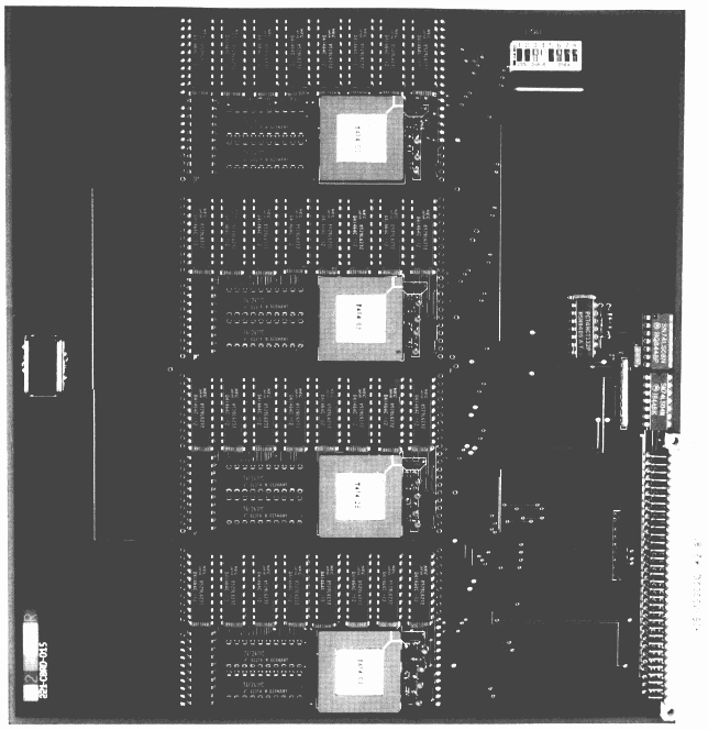
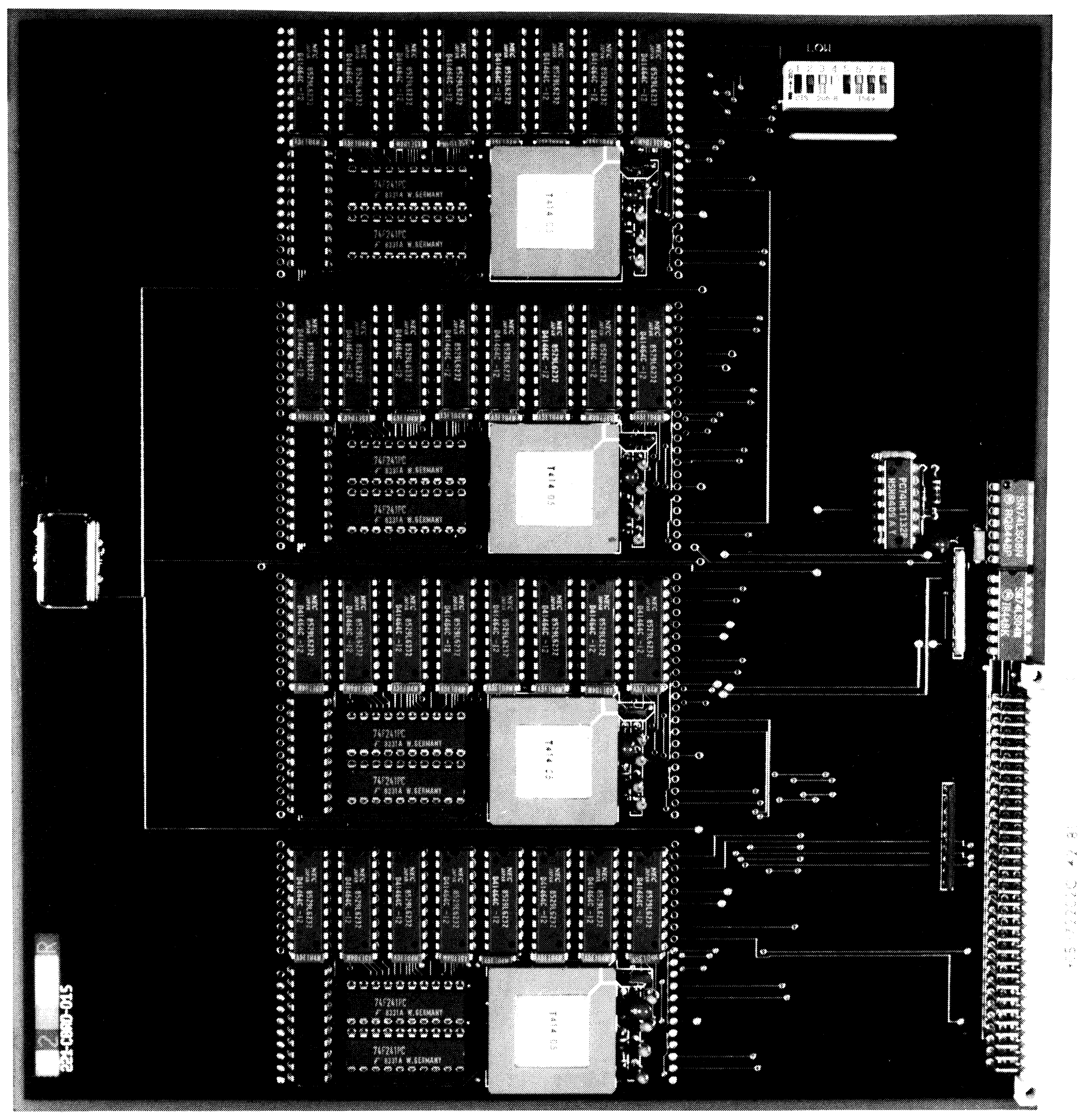
The B003 evaluation board, Figure 1, is a double extended Eurocard containing four T414 transputers, each with 256 Kbytes of dynamic RAM. The four transputers are configured in a square, and two links from each transputer are brought to the edge connector.
The interface from the B003 is via a 96 way DIN 41612 edge connector. Links 0 and 1 from each transputer are brought out via the edge connector together with the system services signals. The connector is a simple superset of the 64 way connector used by B001, B002 and other INMOS evaluation boards.
The board uses a minimum of glue logic. The system services shared by all the transputers consist of a single 5 MHz clock and three packs of TTL. Each transputer uses a further three packs of TTL to interface to its eight RAM chips. The minimal glue logic introduces minimal access time overhead for the RAM, and the T414-15 completes a memory access in four processor cycles.
The square connection of transputers makes it possible to test the board down a single link, minimizes edge connector pin count, and makes it possible to build a wide variety of networks.
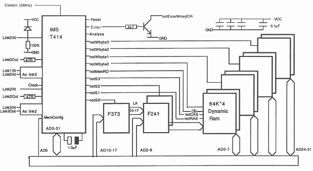
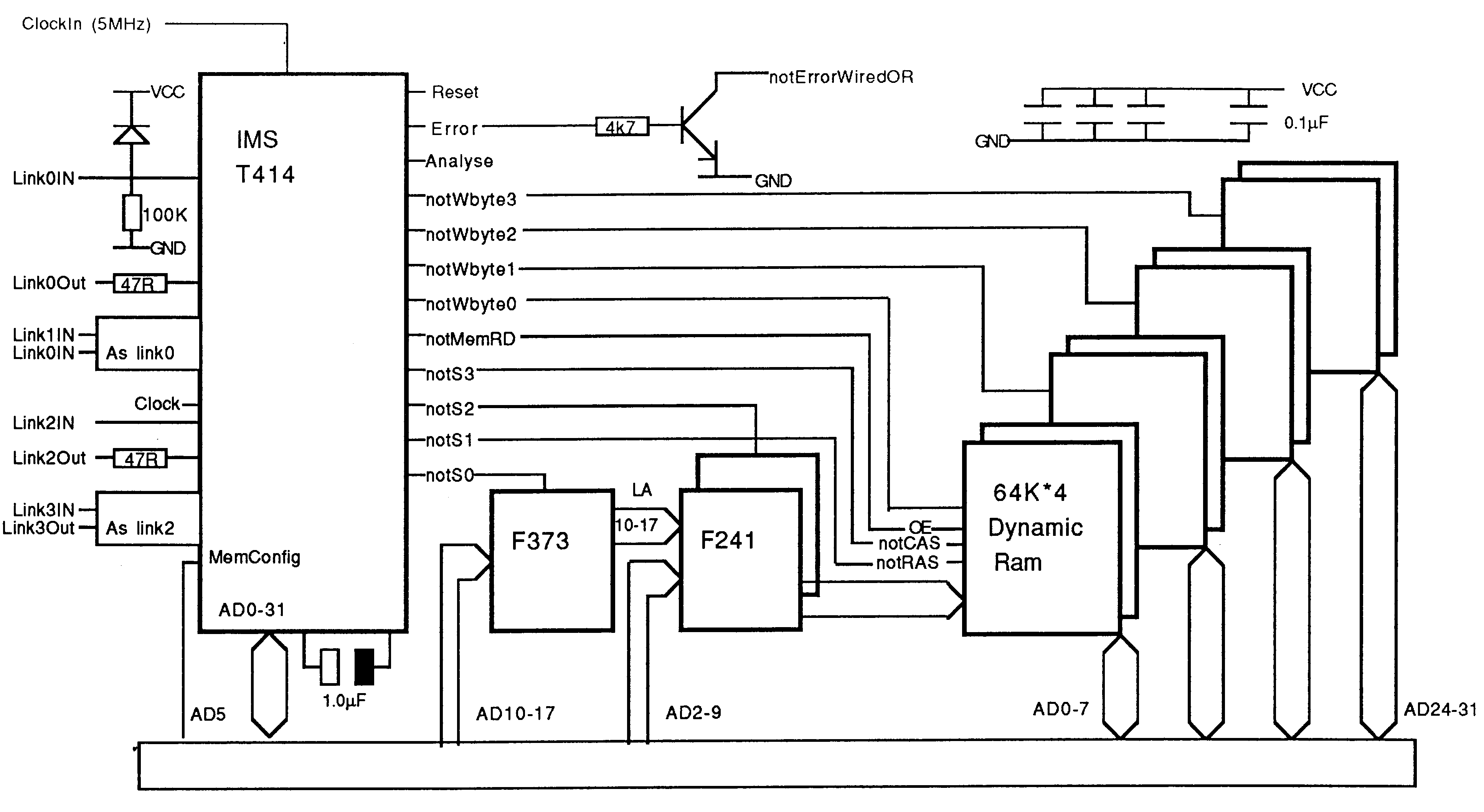
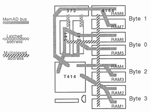
The logic for each transputer with its 256 Kbytes is shown in Figure 2. The RAM is provided by eight 64K*4 dynamic RAMs, with just three TTL packs between the transputer and RAM. Apart from the RAM and TTL, there are a few discrete components for the links, for error, and for decoupling.
The logic is used to latch the column address and to multiplex between the row address and column address.
The load on the F241 multiplexers is sufficiently small (50 pF), and the RAMs are sufficiently close to the F241 outputs that series matching resistors are not needed.
The control signals RAS, CAS, OE and WEn are taken directly from the transputer signals notMemS1, notMemS3, notMemRd and notMemWByten. No buffering is needed because the transputers can easily drive the 50 pF load, and again no series matching resistors are required because the transputer is so close to the RAMs.
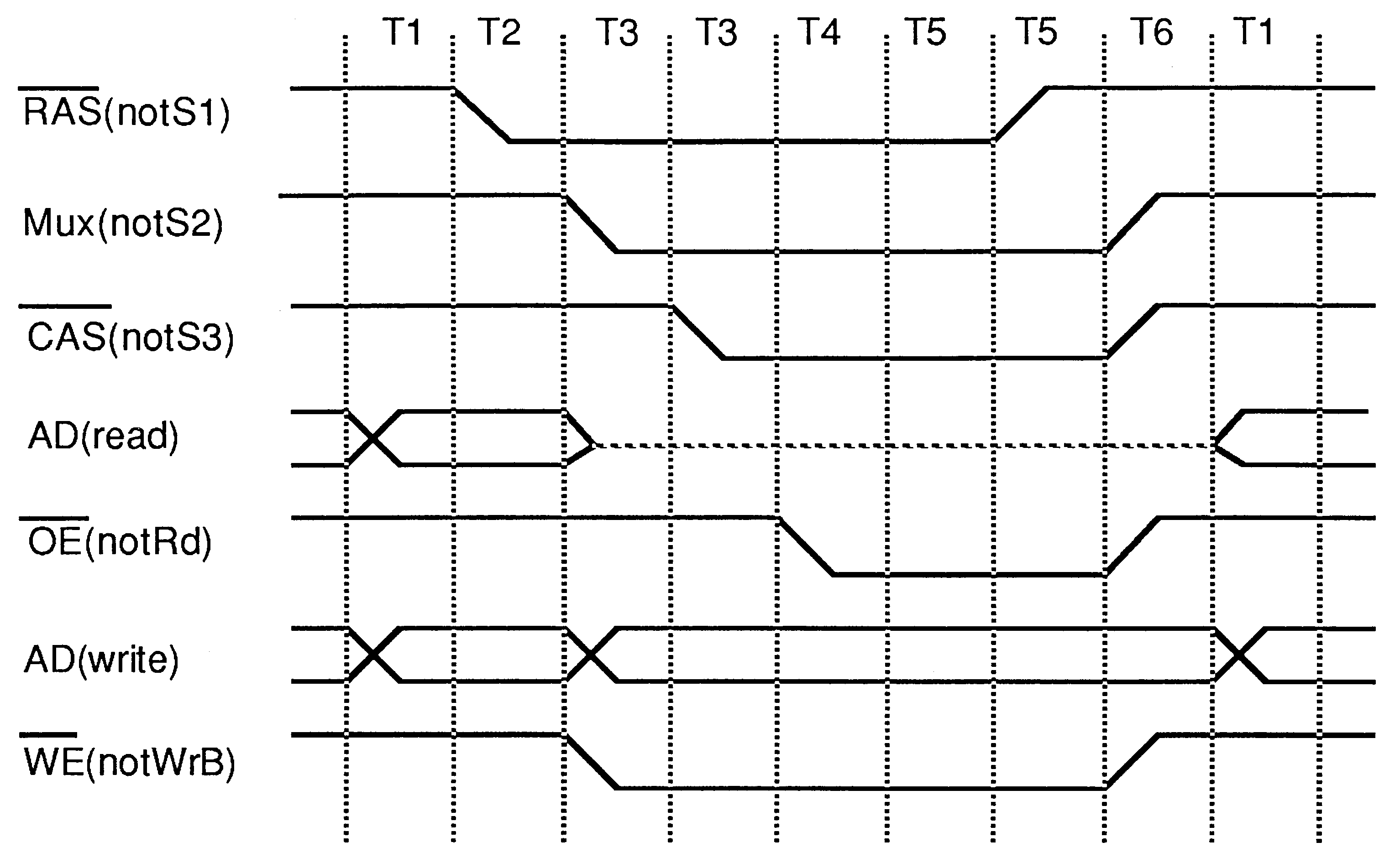
Using such a small amount of logic between the transputer and the RAM not only minimises cost, but also minimises delay. The RAM can therefore be used with minimal overheads on its access and cycle times. The timing diagram for the interface is shown in Figure 3.
Starting RAS at the earliest opportunities and latching the read data at the latest opportunity gives ample margin on access time from both RAS and CAS. Terminating RAS early gives an adequate RAS pulse width, and at the same time ensures sufficient precharge time.
Four processor cycles are used with the T414-15 and the 41464-12 RAMs because the cycle time of the RAM, at 220 ns, is more than would be provided by a memory interface cycle of three processor cycles.
The links of the transputer used on the B003 are capable of running at 20 Mbits/s, at which speed they will not tolerate skew introduced by buffering.
Links 2 and 3 of each transputer which are connected within the B003 have a simple series termination on the LinkOut signal. The termination resistor of 47 ohms, combined with the output impedance of the LinkOut circuit, gives a termination impedance marginally below 100 ohms.
Links 0 and 1, which are brought to the edge connector, also have 47 ohm resistors on the link outputs. The link inputs also need pull down resistors in case a link is not connected. On the transputers used on the B003, the link inputs are more sensitive to electrostatic discharge (ESD) than the link outputs, and so the link inputs which connect to the edge connector are protected by schottky diodes; with the diodes the transputer can withstand ’zap’ tests of up to 2 kV without damage.
The error output produced by the transputer is active high, which is suitable when there is one transputer on a board but causes extra wiring and logic if there are many transputers on a board. To simplify the wiring, a notErrorWiredOR signal is generated by a resistor and transistor.
The power supply decoupling for the RAM and for the TTL is so close to the transputer that it provides excellent decoupling for the transputer. In addition to the power supply decoupling a further capacitor is needed between CapPlus and CapMinus to decouple an internal power supply used by the phase locked loop/clock multiplier. This capacitor was originally a 10 uF tantalum capacitor, but has been changed to 1 uF ceramic for future production.
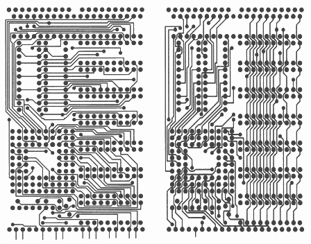
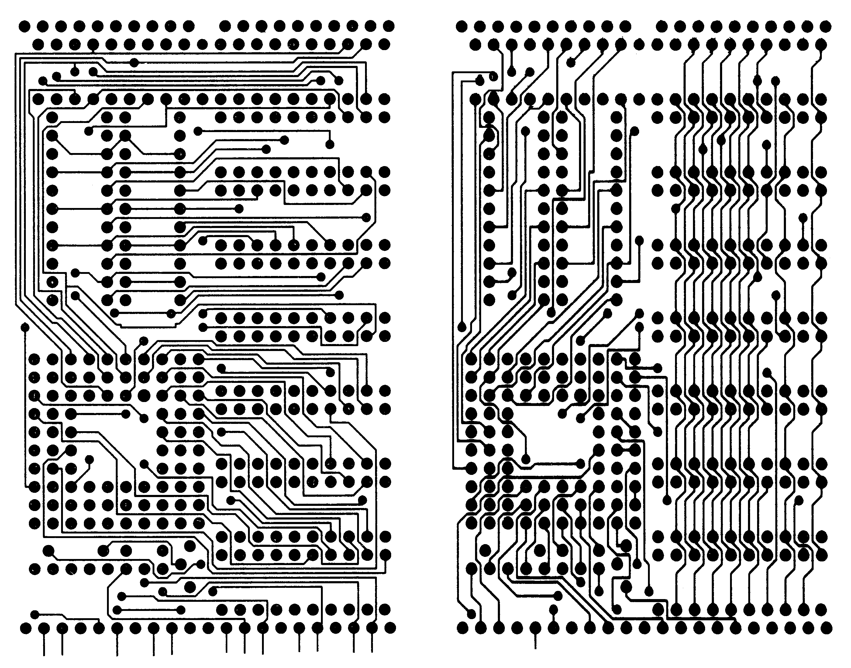
The printed circuit is a straightforward 4 layer board with power and ground planes for the inner layers, and all signal traces on the outer layers. The design rules are an easily manufacturable 0.010” trace, with 0.008” between traces. Component pads are 0.070”, with 1 mm holes; vias are 0.050” pads with 0.6 mm holes. Only one trace is allowed between pads.
The two outer layers are shown in Figure 5.
PGAs have been somewhat notorious for the difficulty they present to PCB layout. At first sight this layout appeared difficult, but careful component placement and orientation resulted in surprisingly simple layout, and there is still transparency for a number of additional connections.
Aspects of the placement which helped were:
∙ moving the link and control connections so they do not interfere with the memory connections;
∙ placing ICs lengthwise to the transputer. This allows maximum transparency, without pads getting in the way;
∙ moving the 373 to beyond the address multiplexors, which also had the effect of putting Byte 1 of the RAMs beyond Byte 0.
Overall signal flow is shown in Figure 4:
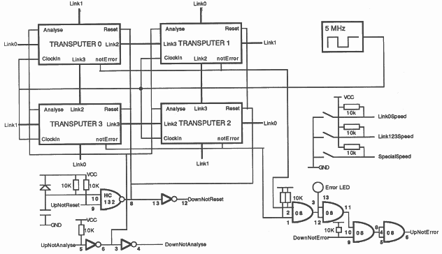
The logic shared by all the transputers is shown in Figure 6.
The evaluation boards share a common system control architecture. The aim of the system control functions is that it should be possible to control an arbitrarily large system built with the boards. The control implies the ability to reset the system, to note that an error has occurred in the system, and to analyse the error. Signals are provided for this purpose in the Up and Down sockets on the edge connector.
Up and Down sockets of evaluation boards are connected in a daisy chain as shown below. The board at the top of the chain is controlled by a Subsystem socket on another evaluation board. The Subsystem socket has the same signals as the Up and Down sockets, but the Subsystem signals can be controlled by software running on the board with the Subsystem socket.
The Reset and Analyse signals flow in the direction of the arrows shown below, the Error signal flows in the reverse direction from Down to Up, and indicates that an error has occurred on this board or on a board further down from this board.
All the B003’s transputers are reset on power ON. A single Error LED (yellow) lights if an error has occurred on this board.
The coding switch sets the Link speed signals for all the transputers. Separate controls are provided for Links 0 and Links 123, which are independently set to 10 Mbits/s or 20 Mbits/sec.
The board uses a single 5 MHz clock oscillator, which is shared by all the transputers.