|
|
| IMS B010 NEC add-in board _____________________________________________________________________ |
| Pete Moore April 1987 |
The INMOS transputer family is a radical new approach to microprocessor design. To help potential users to understand the operation of transputers (and appreciate their performance) a range of evaluation boards have been produced. These allow fast ’hands-on’ experience of transputers and occam, the concurrent programming language developed by INMOS to fully exploit the parallel processing inherent in the transputer architecture.
The IMS B010 is designed to fit into the expansion slot provided on the NEC range of personal computers. In this respect it is comparable to an earlier product, the IMS B004, which fits into the IBM PC.
The NEC PC-9801 family has a dominant market share in Japan and the IMS B010 has been specifically designed to make transputers easily available to this market. The board and development software can be installed and used within a matter of minutes, thus relieving the user of the long and expensive task of initial hardware development.
|
|
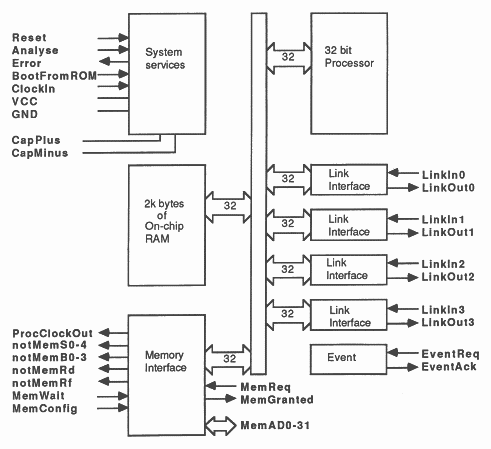
The T414 transputer used in the IMS B010 is a complete computer on a chip. There is a 32 bit processor (capable of 10 MIPS throughput), a small amount of fast (50ns cycle), on-chip static RAM, four serial communications links (for external communications), and a programmable external memory interface. The block diagram is shown in figure 1.
The 32 bit multiplexed address/data bus of the T414 allows up to 4 GBytes physically addressable memory, external to the transputer, as well as the 2 KBytes fast static RAM on board the transputer itself. The memory map of the transputer is signed, with the internal RAM starting, at the most negative address (Hex 80000000 to Hex 800007FF). The external memory starts at Hex 80000800.
The transputer, and the programming language occam, evolved together. Occam was designed to simplify the task of concurrent programming. Occam consists of three primitive processes, which are combined to create larger processes.
| v := a | assign the value of expression a to variable v |
| c ! e | output expression a to channel c |
| c ? v | input a value from channel c into variable v |
These primitives are combined to create processes using the occam constructors:
| SEQ | operate on the component processes in sequence |
| PAR | operate on the component processes concurrently |
| ALT | operate on the first process to become ready |
IF and WHILE constructs are also available. Each constructor is itself a process, and can be used inside other constructors to create larger processes. Concurrent processes, which cannot use shared resources, communicate across occam channels. These channels are single direction, point to point connections between processes, and give synchronised message communication.
Concurrent programming evolved as it became clear that many programs could be split into a number of tasks which could be operated on independently, and use some form of communication for passing results, parameters, and synchronisation.
On standard sequential machines, concurrency has been simulated by making the processor share its time between each task. This required a complex software ’kernel’ to be written, which would control the switching of tasks (including itself) in and out of the processor, and handle the passing of messages. Switching the tasks frequently gives the user the impression that all of the processes are running simultaneously.
When developing occam programs on host machines such as the Personal Computer, an occam kernel is supplied to implement the concurrency and message passing via occam channels.
On transputers, the kernel has been implemented in hardware, giving a sub-microsecond task switch time, compared to a few milliseconds on software driven multitasking machines. Occam processes can be mapped onto one transputer, which shares its time between them, or onto multiple tranputers, each taking a subset of the processes. The occam channels are mapped onto the transputer links for processes on separate processors. In this way, programs can be developed on a single transputer, and extended to multiple transputers as more performance is required.
The transputer’s links operate at 10 MBits/sec, full duplex. Each link is capable of supporting two occam channels, one into the transputer, and one out from the transputer. Links are implemented as autonomous DMA (Direct Memory Access) engines, and so can perform communications with external devices as background tasks to the processor with negligible performance degradation.
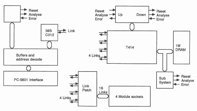
The IMS B010 has three distinct elements (as shown in figure 2).
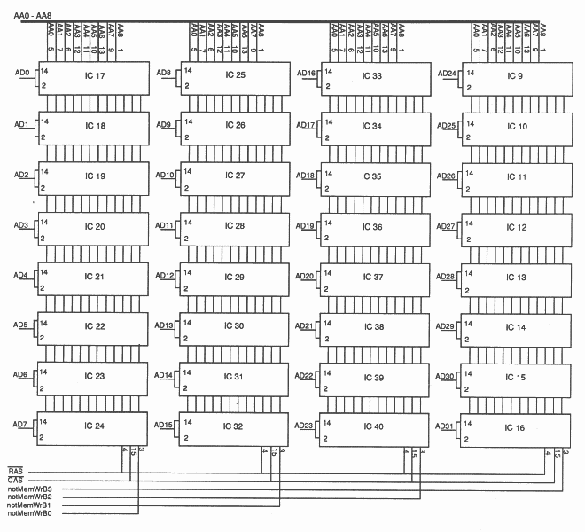
The transputer used is the T414, a 32 bit processor, with 1 Mbyte of external RAM. To enable this amount of RAM to be fitted onto the NEC form-factor board, 256Kbit dynamic RAMS (32) were used, giving four banks of 256kBytes each. There is no parity checking.
The interface to the NEC Personal Computer uses an Inmos link adapter, which converts the serial data from an INMOS link into byte-wide parallel data, and vice versa. The device is memory mapped into the NEC I/O address space and appears to the PC as a group of 4 registers.
There is another group of registers in the I/O address space which are associated with the system control, namely reset, analyse and error. These allow the host PC to control the transputer subsystem and service error conditions.
The three functional blocks are connected together by jumpers on a 96 way connector. The interface and control blocks may be selected to be inactive, and the link adapter’s serial link may be connected to any of the transputer’s 4 links. In this way several boards may be used within the same PC with only one selected to be the master. Alternatively, the addresses of the link adapter/control registers may be changed (again by jumpers on the 96 way connector), allowing several boards to control their own subsystems, and to accommodate other manufacturers’ expansion boards which may use similar I/O addresses.
The main functional blocks of the IMS B010 are shown in figure 2.
Much of the logic required to control the board and to decode NEC I/O addresses is implemented in PAL logic. In the design, this logic is described in terms of the programming language CUPL (Universal Compiler for Programmable Logic), available from Assisted Technology.
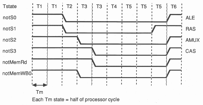
To ease the task of designing memory systems, the transputer has an on-chip configurable external memory interface (EMI). With this interface, it is possible to configure the external memory cycle of the transputer to be any width (to suit slow or fast memories), and a number of programmable strobes are supplied, which can be programmed to give signals such as notRAS and notCAS for dynamic memories. Automatic refresh, over a selectable refresh cycle time, can also be chosen. This eliminates the need to design complex timing generators, and so cuts down the number of devices required on the board.
The external memory cycle is split into six states. These ’T states’ are as follows :
| State | |
| 1: | Address set up |
| 2: | Address hold |
| 3: | Read cycle tri-state/write cycle data setup |
| 4: | Extended for WAIT states |
| 5: | Read or write data |
| 6: | End tri-state/data hold |
The configuration of the memory cycle consists of specifying the number of each of these states that are required to give the timing needed by the particular memory device used. The memory interface is programmable to a resolution of a period ’Tm’, where Tm is the time for half a processor cycle. Any T State can consist of one to four Tm periods (The transputer has a Wait input which can be used to selectively insert more T4 states). The user programmable strobes are also defined with reference to Tm. A program is included in the transputer development system for calculating the configuration with reference to the memory device data sheets.
The transputer has a number of pre-defined configuration patterns that can be used. During the initial reset phase, the transputer scans the MemAD pins to see if any are connected to MemConfig. If so, an internal configuration is chosen, otherwise the user must supply the configuration data as described in the transputer manual [1].
The IMS B010 uses RevB transputers, with a 50ns processor cycle, and the DRAMS used have access times of 100ns. The memory interface can be correctly configured by connecting the MemConfig pin to AD6.
Early write cycles are used so that the Din and Dout pins of the DRAMS can be commoned, and there is no need for buffering the data bus.
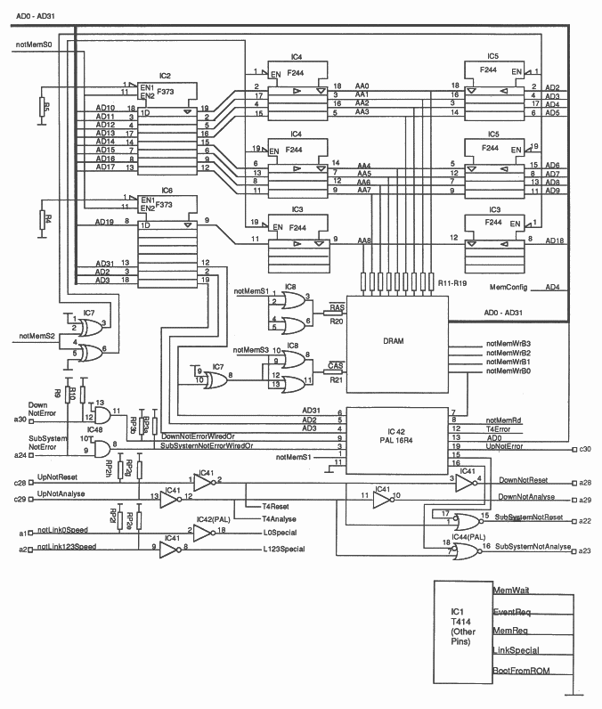
Once the memory interface has been configured correctly, the logic for controlling the memory must be designed. As the memory interface controller on the transputer generates all of the signals needed, the only logic required are buffer and latch devices, used to multiplex the Row and Column addresses, and to drive the chips in the memory array.
The transputer memory bus is a 32 bit, multiplexed address/data bus. The address is output during 12, and so we must latch the signals we require for the rest of the cycle. Because word addressing is used, successive addresses are spaced apart by increments of four. This leaves MemAD0 and MemAD1 free during address generation, so they are used to carry information related to the type of cycle that is being executed. MemnotWrD0 signifies a write cycle when active, MemnotRfD1 signifies a refresh cycle.
For this memory system, we do not need the MemnotRfD1 signal. When notRAS goes low on a refresh cycle, the value present on the address lines A0-A7 is used to decode the row to be refreshed. During a refresh cycle the transputer outputs the value of its 10 bit refresh counter onto AD2-AD11, with all other AD lines high.
AD31 is inverted and OR-ed (IC8) with notMemS3 to produce the notCAS signal to the DRAM array. The signal notRAS is taken directly from notMemS1; the two spare Or gates in IC8 are used simply to provide more drive capability, as there are 32 memory devices on the board.
Two F373 transparent latches (IC2 and IC6) are used to capture the signals needed for the column address, the latches being enabled by the falling edge of notMemS0 at the start of T2. At this point, we can be sure that the addresses are stable on the bus. At the same time, we can strobe in the row address (the low order address bits present on the bus during T2 and buffered by IC5 and IC3) to the DRAMS, using the notRAS signal derived from notMemS1.
Once the row address has been latched by the RAM, the column address (stored by the latches) must be presented to the RAM address inputs. The latches have limited drive capability and must be buffered (IC3 and IC4).
When stable, the column address can be strobed in, using notCAS. The signal notMemS2 is used to perform the switching of the row-column addresses; IC7 is used to ensure the two buffer strobe signals are non-overlapping.
The circuit for the memory decoding is shown in figure 4, and the memory array itself is shown in figure 5.
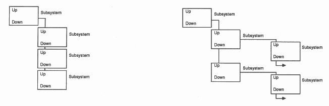
The board architecture, common to all INMOS transputer evaluation boards, allows any number of boards to be connected together to create a multi-processor system. On each board, the transputer links are brought to the edge connector, and cables are used to interconnect transputers on separate boards.
A number of control signals are also brought to the edge of the board, to provide control over the transputer’s reset, analyse and error functions. The system control signals are standard throughout Inmos transputer evaluation boards, and to understand the needs for the hardware to implement these control lines, the system architecture of the boards needs to be examined. Figure 6 shows how a hierarchical network of boards can be built into a large system.
The Up, Down, and Subsystem ports all carry the same control signals. These are:
The notReset and notAnalyse signals flow down the system (if the configuration of the system is considered to be as in figure 6), while the notError signal flows upwards. The notAnalyse signal is used to place the system into Analyse mode (see [1]).
For the IMS B010, there are two paths we must look at.
The propagation of these signals is further modified on the IMS B010 by the inclusion of sockets to accept future expansion modules. These may be connected (via jumpers) to either the down or the subsystem control ports.
The schematic of the control system is shown in figure 4.
The architecture allows for any board in a chain to act as a master for another chain, allowing large systems to be split up into smaller subsystems, each with its own local controller. If an error occurs in the system, it can be handled by the local controller, without interfering with the rest of the system.
The transputer subsystem signals are handled by the 16R4 PAL IC42. The subsystem control is done via registers in the transputers positive address space (The addresses given are WORD addresses):
| SubsystemReset (write only) | Hex 0 |
| SubsystemAnalyse (write only) | Hex 4 |
| SubsystemError (read only) | Hex 0 |
Writing a ’1’ to bit 0 of SubsystemReset or SubsystemAnalyse asserts the associated signal, a ’0’ clears the signal. If bit 0 of SubsystemError is set, an error has been detected. SubsystemReset and SubsystemAnalyse are also asserted when their respective Up signals are asserted, thus a top level reset or analyse (for instance at power-on) will ensure that all parts of the system are correctly reset. The logic required for these functions is described in appendix A.
The logic required for the Up and Down ports is simple. The UpnotReset and UpnotAnalyse for the daisy chaining of boards enter the board from the Up port, are inverted (IC41) to give the correct polarity for the transputer Reset and Analyse, and are then inverted again for output at the Down port. The second inverter is used to provide the drive current required between boards. Both inputs (from the Up port) are pulled high with 1K resistors to prevent spurious resets occurring when no external boards are connected.
The DownnotError and SubsystemnotError signals are both inverted in IC48 (again, a 1K pull up resistor is used to hold the line at the ’no error’ state when no other boards are connected). IC48 is an open-collector device, thus enabling us to ’Wire-Or’ the outputs; this is necessary when connecting expansion modules to the board (see section 4.2). These two signals and the transputer error are combined in IC42 (16R4 PAL) to generate the UpnotError. The logic required to do this is given in appendix A.
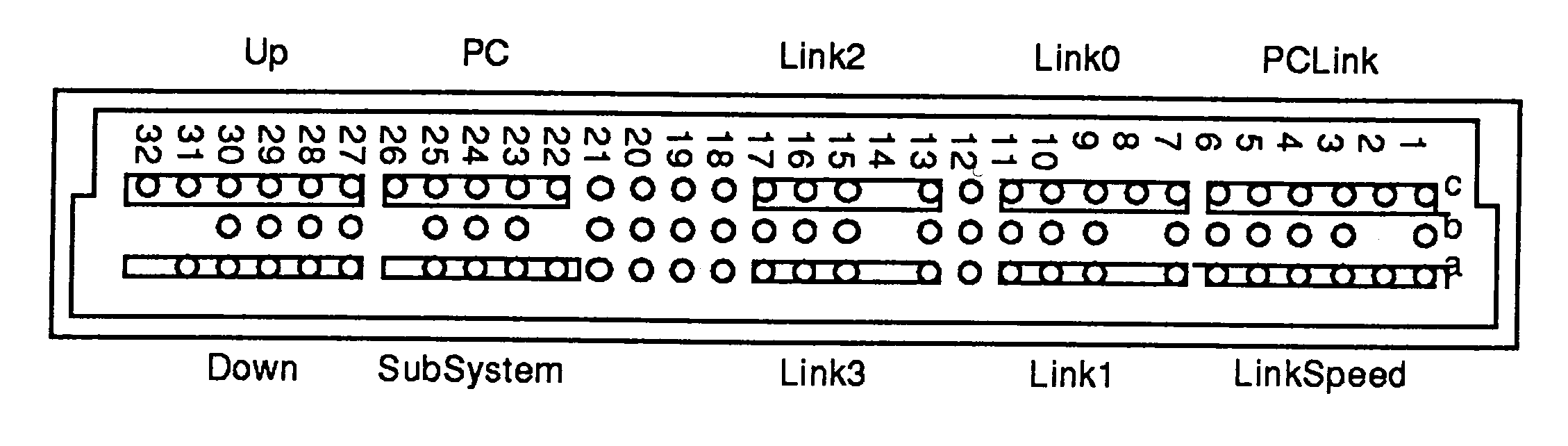
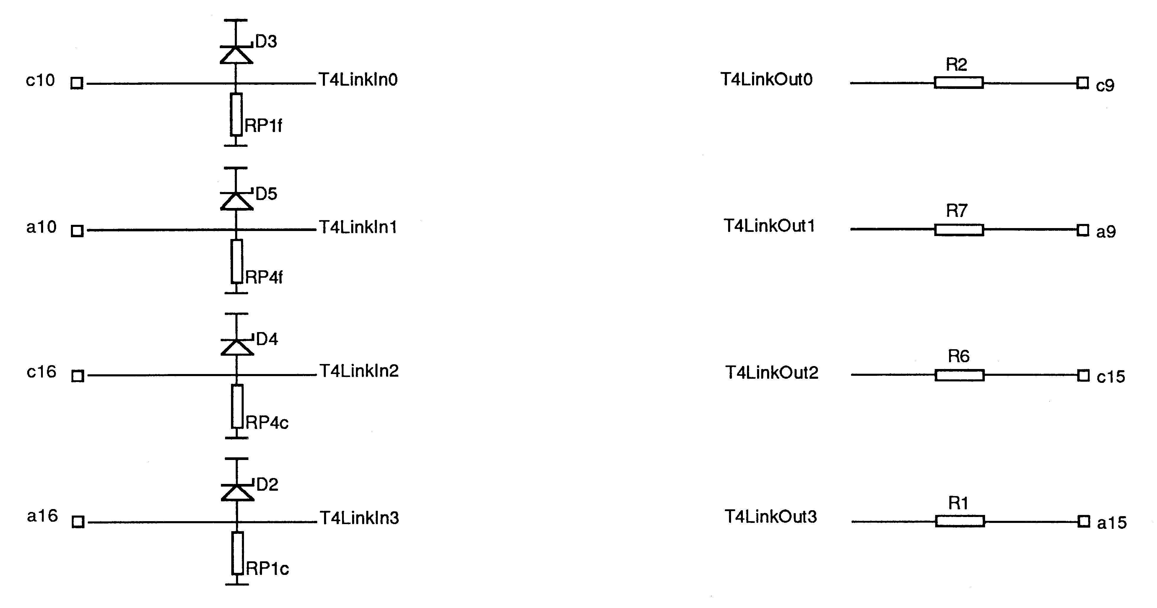
All of the links and control ports are accessed from a 96way connector on the edge of the board, and are arranged in groups of five. This fits the standard adopted for all INMOS evaluation boards and allows different boards to be interconnected. The arrangement of signals and polarising keys on the cables makes it difficult to cross links and control ports. The signals on the 96way connector are shown in figure 7.
The transputer and link adaptor have link speed selection pins. These are controlled by two signals on the 96way edge connector which are normally held high by resistors. They are inverted (IC41 and IC42) to give default link speeds of 10 MBits/sec. Pulling link0special low will change the speed of the transputer link0 and the link adaptor to 5 MBits/sec; link123special will have a similar effect on the transputer links 1 to 3. The linkspecial pin is held to ground; if held high the links are switchable between 10 MBits/sec and 20 MBits/sec.
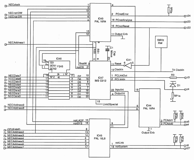
The task of interfacing the NEC PC parallel I/O bus to the transputer is handled by another INMOS device, the IMS C012 link adapter. This converts byte wide data into serial form for communicating via a standard INMOS link. The device appears as a memory mapped peripheral in the I/O address space and has four registers; these contain input and output data as well as separate input and output status registers. A number of standard control lines, such as chip-enable, read/write and register select are included and there are transputer compatible clocks, reset and link speed selection. The operation of the device is described in detail in the transputer reference manual [1], see also [2]).
This approach offers advantages over a conventional interface which is located within the transputers memory map:
The only disadvantage with this method is that one of the transputers within the system has a link permanently dedicated to host communication. This is not usually a problem.
The circuit to perform the communications with the Personal Computer is outlined in figure 8.
Also included in the PC interface are more system control signals, which operate in the same manner as the transputer subsystem signals, but controlled by the Personal Computer. This allows the PC to be the master system controller. To allow more than one evaluation board to be fitted within a host, a method of selecting only one link adaptor and system control circuit to respond to accesses by the host was required. This selection method would allow all other boards to have all four links available for general use.
To satisfy these needs, it was decided to take the link from the link adaptor to the rear of the board, and to use a jumper plug to connect a transputer link to the link adaptor. A mechanism is included which informs the decoding logic that the jumper plug is in place, and the board can respond to the PC. The system control signals (controlled by the PC) are also taken to the rear connector, using a jumper plug to connect to the Up port, and using a similar selection mechanism to the links.
The selection mechanism requires an input of the selection PAL (IC45) to be pulled low (normally pulled high with resistors) if one of the jumper plugs is inserted. Only if the line (notLink or notSystem) is low will the corresponding select signal (notLADP or notSYS) be asserted. This signal enables the logic in IC43.
The address at which the board resides is also controlled by jumpers on the 96way connector. The two input lines PCAdd0 and PCAdd1 are pulled high by 1K resistors, and if either of them is taken low cause IC44 to include A8 and A9 in the address decoding, feeding an enable signal to IC43. The actual addresses thus decoded are given in the following table:
| PCAdd1 | PCAdd0 | I/O Address (decimal) |
| 0 | 0 | 208 to 219 |
| 0 | 1 | 464 to 475 |
| 1 | 0 | 720 to 731 |
| 1 | 1 | 208 to 219, 464 to 475, |
| 720 to 731, 976 to 987. (ie Don’t care) |
The NEC address decoding is done by IC45, a 16L8 PAL. A2 to A7 are decoded, as well as CpuEnbl0, and this generates two control signals notLADP and notSYS (conditional on the correct inputs to notLink and notSystem).
If notSYS is asserted, IC43 will allow the PC to access the registers used to control the Reset, Analyse, and Error signals. These registers operate in a similar manner to the subsystem control registers.
Writing a ’1’ to bit 0 of PCReset or PCAnalyse asserts the associated signal, a ’0’ clears the signal. If bit 0 of PCError is asserted, an error has been detected.
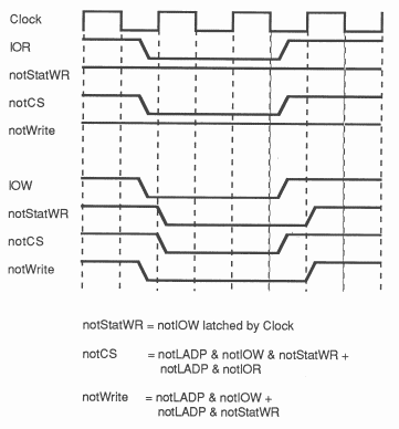
notLADP is used to select the link adaptor timing logic in IC43. Here, the NECnotIOW, NECnotIOR, and NECclock signals from the PC bus are used to generate the access timing sequence for the link adaptor, as shown in figure 9.
Chip-select (notCS) and the write strobe (notWrite) are also used to control the enabling and direction of the bi-directional buffer IC46 (LS245). Note that notPCReset (after being inverted) is also used to reset the IMS C012. This ensures that all links are reset before loading of the system takes place.
The four link adapter registers are decoded by the IMS C012 using Al and A2 as the register select lines. The clock input is 5MHz; the device, in common with transputers, has an on-chip phase locked loop to multiply the clock frequency locally. Thus many transputers/link adapters may be driven by a single (relatively slow) clock which is easy to route around a PCB; there is no problem with relative edge rate timing as all devices run asynchronously.
The link circuitry is also shown in figure 8, and the transputer links are shown in figure 10. When connecting links together it is not necessary to buffer them, although all output links have a series termination resistor (47ohm). Link inputs have pull down resistors (100Kohm), which are used to prevent noise on the inputs to unused links which may be interpreted by the transputer as code or data. All link inputs have a diode connected to Vdd. This serves two purposes, firstly as a protection against static charges, and secondly to prevent latch-up should the device be unpowered when connected to a ’live’ board.
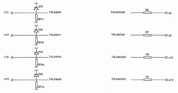
At this point the concept of transputer modules may be introduced. These are small PCBs designed to hold a transputer and some external memory. They all share a common shape and size, or multiples thereof (depending on how much memory etc), and allow the user to plug them into prototype or mother-boards with little hardware design effort. There are nominally 16 pins carrying the following signals:
The IMS B010 supports transputer modules; there are sockets on board to take up to four standard size modules (the first of which will have 32kBytes of DRAM), or one ’quad’ size module (which is actually derived from the layout of the IMS B010 transputer and memory). Provision has been made to patch any of the 16 extra links to each other, or to four extra link sockets (W,X,Y and Z) on the 96way connector, using wire-wrap d.i.l. headers in LP1 and LP2.
The modules may be connected to the IMS B010 subsystem port, or to the down port, by means of three jumpers located near to the 96way connector. As we have already seen, both subsystem and down error signals are driven by open collector devices. The transputer modules have an open collector transistor on board, so these signals are simply ’Wire-Ored’ together. The reset and analyse signals to the modules must be inverted; this is done by IC44. This circuit and the jumpers are shown in figure 11.
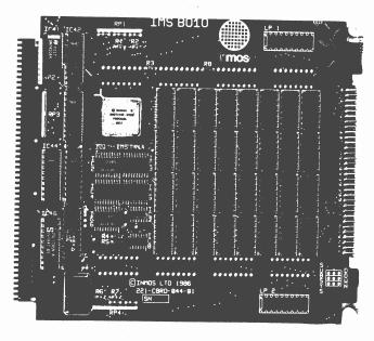
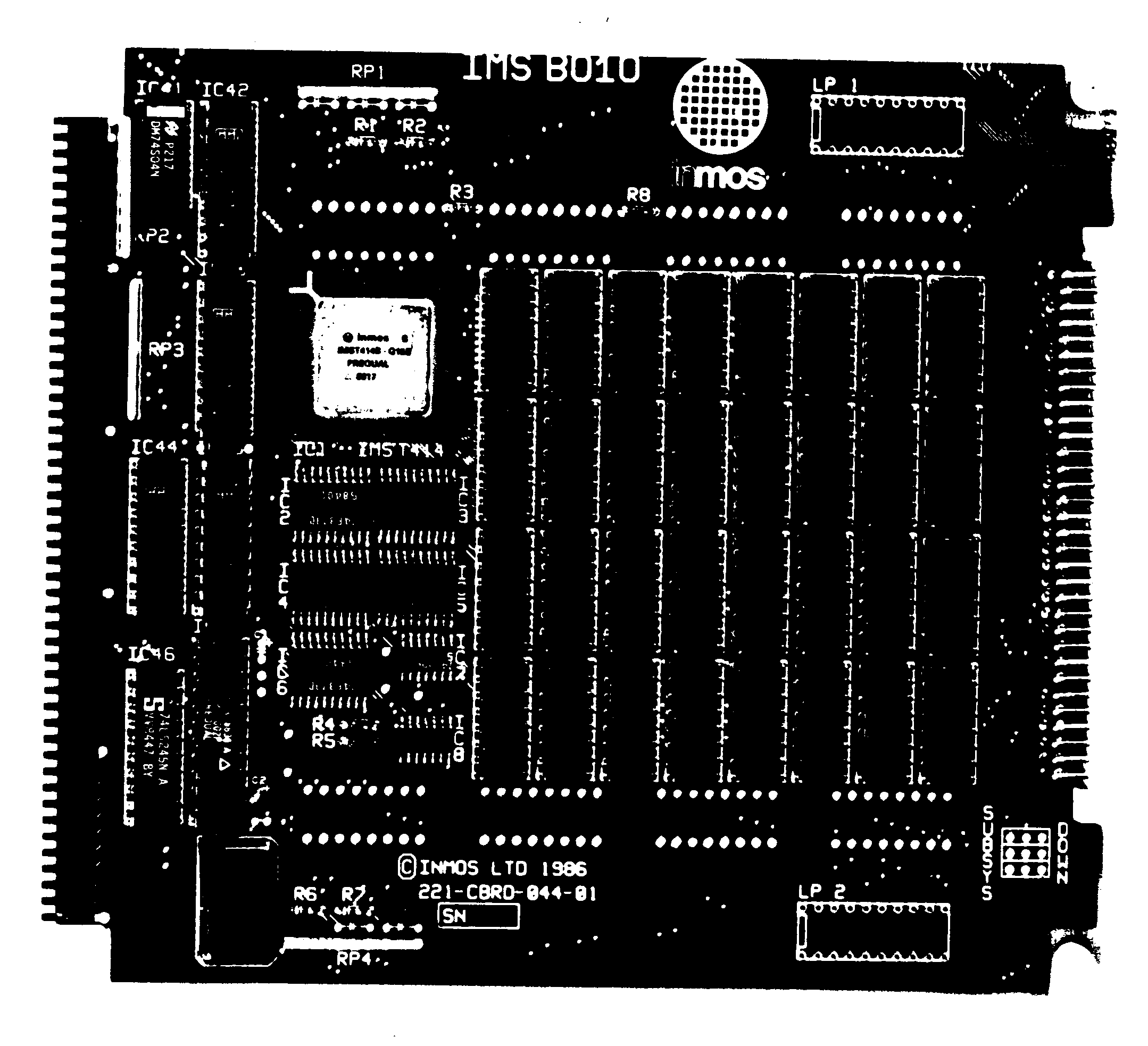
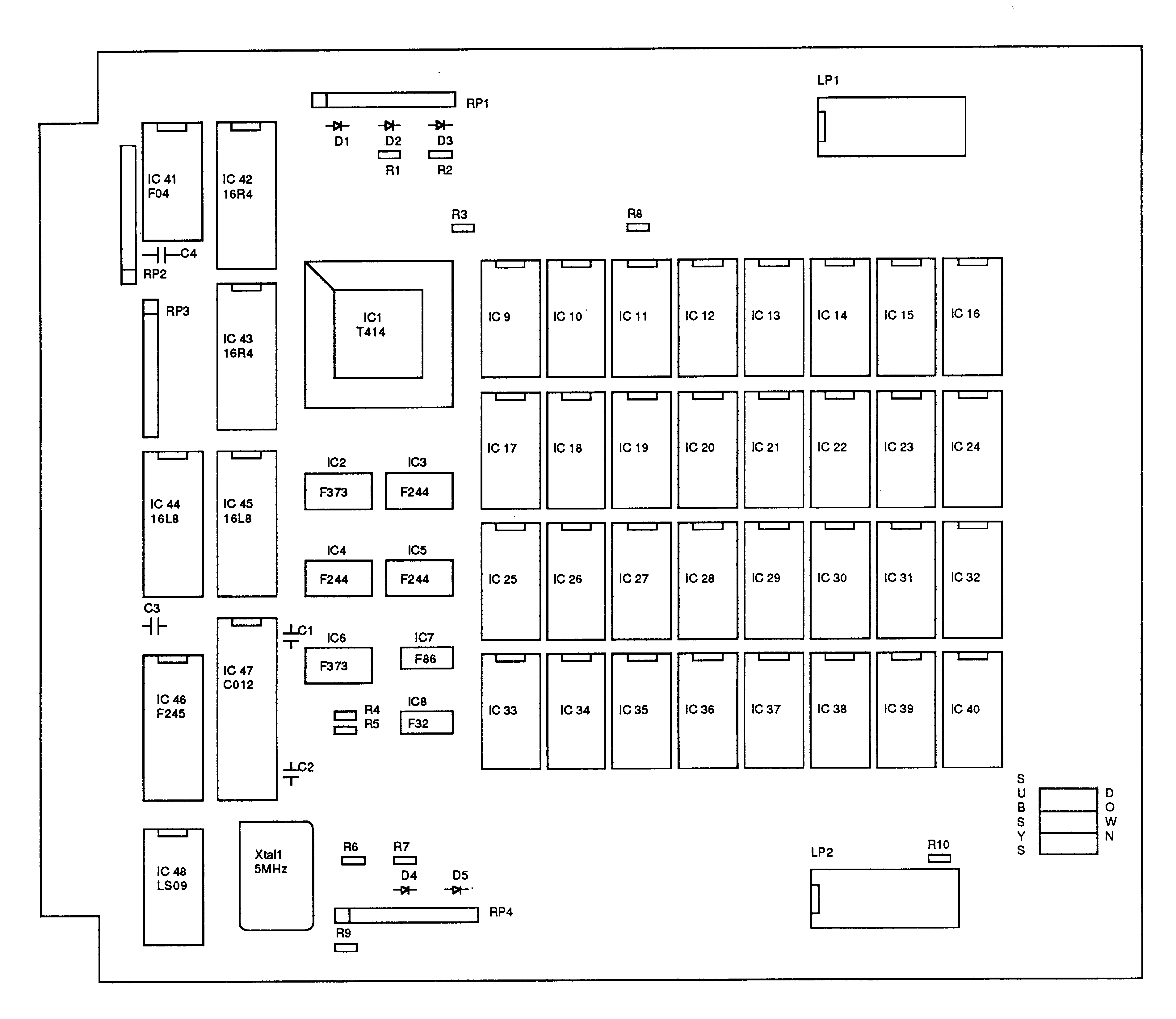
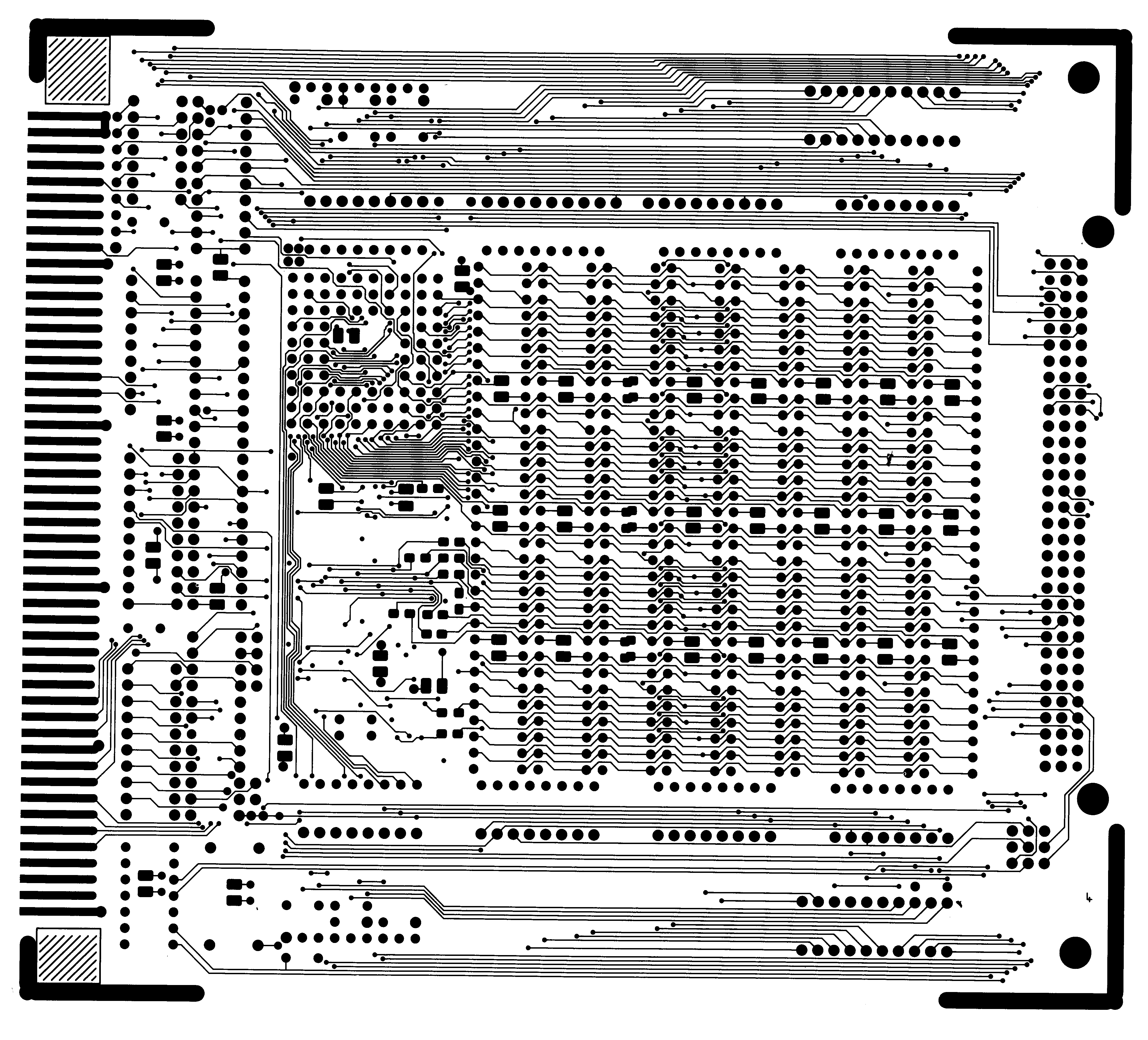
The IMS B010 is a four layer printed circuit board (PCB) with a gold-plated edge connector along one edge, and measuring 168mm by 148mm (NEC expansion slot form-factor). The 96way connector for the links and control ports is on the opposite edge of the board, and there are mounting holes for NEC-type card extractors.
It was decided at a very early stage of the design to try to fit the transputer and 1 MByte of DRAM into the space taken up by four INMOS transputer modules, thus allowing the layout to be lifted and modified to make a module. To facilitate this, it is necessary to use small outline (SO) surface mounted packages for the seven memory latch and driver devices (IC2 to IC8).
All other ICs are mounted in sockets. For ultra-low component profile, through-board IC socket pins are used, allowing transputer modules to be mounted above the PCB. Decoupling capacitors (approximately one per IC pack) are of the surface mounted ’chip’ type.
With such a high packing density around the transputer it is necessary to use tight design rules, notably track widths of 0.008 inch and inter-track spacing of only 0.007 inch. There are only two signal layers, with two tracks between IC pads. The via holes used are 0.5mm diameter. Two layers of interconnect are used, the inner layers being reserved for ground and Vdd planes (past experience shows this arrangement gives good decoupling and signal fidelity).
The board area outside of the main transputer module is relatively low density; the PC interface logic resides close to the NEC edge connector with the remainder taken up by interconnect, the extra module links taking a large proportion.
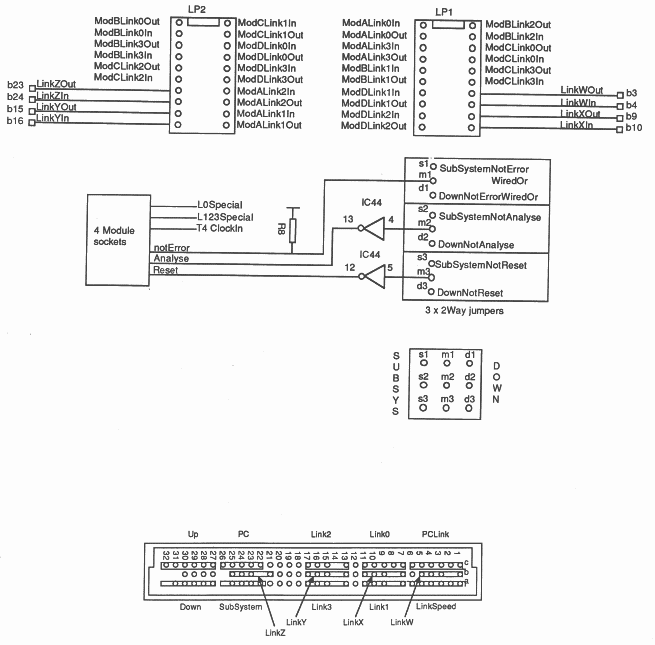
The component layout is shown in figure 12. The component list and PCB layout is given in appendix B.
As the transputer can be programmed to supply all the timing signals necessary to build an external memory system, the design of a transputer system consists mainly of latching and buffering address, data, and control lines to provide sufficient drive current for the board. Practical things to note are the use of pull up or pull down resistors on all inputs of the board. Output links have a series resistor used for line matching (approx 47ohm). The input links require pull down resistors (approx 100Kohm), to prevent floating inputs from being interpreted as code or data. All of the control signals (Up, Down, and Subsystem) are active low, so pull up resistors are required on all inputs to the board, to prevent unused lines floating.
All devices should have adequate decoupling capacitors; if possible 100nF ceramic capacitors (one per pack) and a few larger tantalum capacitors (47uF). The transputer requires separate decoupling for its phase locked loop (PLL); a 1uF ceramic is sufficient, placed as close as possible to the device pins (Cap Plus and Cap Minus), but in any case within 1.5 inches of PCB track. Similarly, the IMS C012 requires PLL decoupling,
The interface described is that used to communicate with a Personal Computer bus. The IMSC012 can be interfaced to any parallel bus, with small changes to the timing logic (implemented in a PAL).
The first version of the board exhibited excessive undershoot on the latched memory drive lines, and on notRAS and notCAS. This required series termination resistors which were surface mounted due to the lack of board space. Initially 50ohm resistors were used, but laboratory measurements showed the optimum value for this particular board to be 33ohm.
At the time of initial board development, the IMS C012 was not in full production, so the board was designed to be easily modified to use the IMS C002 link adapter. This is an earlier version of the IMS C012, the only visible difference being the reset and PLL decoupling pins interchanged. This is catered for by cutting a track and moving the position of the capacitor if the older link adapter is to be used. This is not necessary on current production boards.
It is very difficult to give precise performance figures for any system, as so much depends on the algorithm in use. The IMS B010 offers approximately ten times increase in speed over the NEC PC. This may be further increased by adding more transputers and sharing concurrent processes between them. Unlike conventional microprocessors, the processing power increases linearly with additional transputers.
The IMS B010 PC add-in board was primarily designed to complement the Personal Computer as an Occam development station. Any number of evaluation boards can be connected to the board via the links; these may reside within the PC itself, or may be other INMOS evolution boards. The INMOS transputer evaluation module (ITEM) is an ideal environment for developing larger transputer systems, and a range of compatible evaluation boards exists, offering complete flexibility over the number of transputers and size of memory.
Programming the board for specific applications is done using the transputer development system (TDS). The TDS will support programming in occam, ’C’, Pascal, and FORTRAN. With these language compilers, it will be possible to take existing algorithms, and re-compile them for transputer applications. Also, by using occam as the harness to describe the concurrency of the system, it is possible to run multiple processes, which could be written in any of the four languages.
When using the TDS, the host PC acts as a file server, passing data to and from the keyboard, disk and screen to the IMS B010 via the link adaptor.
Other uses include using the board as a high-performance number crunching device, used as a slave processor to the host machine. Here, any application could be written (or a current application modified) to pass data to the board, which will perform certain tasks on that data, before passing it back to the host machine for displaying etc. The interface software sees the board as a number of memory mapped registers. For example, a high performance flight simulator could be written, the transputer system doing the complex trigonometry involved with aircraft position, windowing, 3D-2D conversions, passing vector information to the host computer for display. By using multiple boards, the tasks could be split between many processors, giving orders of magnitude improvement in performance.
The IMS B010 could be used for advanced graphics processing, the results being displayed on the NEC’s own screen.
PARTNO IC42;
NAME IC42; DATE 04/9/86; REV 04; DESIGNER Pete Moore; COMPANY Inmos Limited; ASSEMBLY B010 REV C; LOCATION 16R4; PIN 1 = !notMemS1; /* Register Clock */ PIN 2 = notLink0Speed; PIN 3 = !notSSError; PIN 4 = unusedInput; PIN 5 = A2; PIN 6 = A31; PIN 7 = notWRB0; PIN 8 = !notRD; PIN 9 = !notDNError; PIN 12 = T4Error; PIN 13 = AD0; PIN 14 = nc; PIN 15 = !notSSReset; PIN 16 = !notSSAnalyse; PIN 18 = Link0Speed; PIN 19 = !notUPError; FIELD SelAddr = [A2]; wrReset = AD0 & !A31 & SelAddr:[0] # notSSReset & !(!A31 & SelAddr:[0]); wrAnalyse = AD0 & !A31 & SelAddr:[4] # notSSAnalyse & !(!A31 & SelAddr:[4]); notSSReset.D = notWRB0 & notSSReset # !notWRB0 & wrReset; notSSAnalyse.D = notWRB0 & notSSAnalyse # !notWRB0 & wrAnalyse; Link0Speed = !notLink0Speed; notUPError = T4Error # notDNError; AD0 = notSSError; AD0.OE = SelAddr:[0] & !A31 & notRD; |
PARTNO IC43;
NAME IC43; DATE 13/10/86; REV 03; DESIGNER Pete Moore; COMPANY Inmos Limited; ASSEMBLY B010 REV D; LOCATION 16L8; PIN 1 = NECclock; PIN 2 = !PCNotError; PIN 3 = !notSYS; PIN 4 = B010Enable; PIN 5 = !NECNotIOW; PIN 6 = !NECNotIOR; PIN 7 = A0; PIN 8 = !notLADP; PIN 9 = A1; PIN 11 = nc1; PIN 12 = !RNotW; PIN 13 = !notCS; PIN 14 = !notStatWR; PIN 15 = !PCNotReset; PIN 16 = IPCNotAnalyse; PIN 17 = IntONError; PIN 18 = D0; PIN 19 = ErrInt; FIELD select = [A1..A0]; readsys = NECNotIOR & notSYS & B010Enable; writesys = NECNotIOW & notSYS & B010Enable; readlink = NECNotIOR & notLADP & B010Enable; writelink = NECNotIOW & notLADP & B010Enable; PCNotReset.D = D0 & writesys & select:[0] # PCNotReset & !(writesys & select:[0]); PCNotAnalyse.D = D0 & writesys & select:[1] # PCNotAnalyse & !(writesys & select:[1]); IntONError.D = D0 & writesys & select:[2] # IntONError & !(writesys & select:[2]); D0 = !PCNotError; D0.OE = readsys; notStatWR.D = NECNotIOW; notCS = writelink & notStatWR # readlink; RNotW = writelink # notLADP & notStatWR; ErrInt = PCNotError & IntONError; |
PARTNO IC44;
NAME IC44; DATE 13/10/86; REV 02; DESIGNER Chris Cytera; COMPANY Inmos Limited; ASSEMBLY B010 REV D; LOCATION 16L8; PIN 1 = T4Reset; PIN 2 = PCAdd1; PIN 3 = PCAdd0; PIN 4 = ModuleNotAnalyse; PIN 5 = ModuleNotReset; PIN 6 = nc1; PIN 7 = T4Analyse; PIN 8 = NECSel1; PIN 9 = NECSel0; PIN 11 = nc2; PIN 12 = ModuleReset; PIN 13 = ModuleAnalyse; PIN 14 = nc3; PIN 15 = !SSNotReset; PIN 16 = !SSNotAnalyse; PIN 17 = !notSSResetReg; PIN 18 = !notSSAnalyseReg; PIN 19 = B010Enable; FIELD Select = [PCAdd1..PCAdd0]; FIELD Address = [NECSel1..NECSel0]; ModuleAnalyse = !ModuleNotAnalyse; ModuleReset = !ModuleNotReset; SSNotReset = notSSResetReg # T4Reset; SSNotAnalyse = notSSAnalyseReg # T4Analyse; B010Enable = Select:0 & Address:0 # Select:1 & Address:1 # Select:2 & Address:2 # Select:3; |
PARTNO IC45;
NAME IC45; DATE 14/07/86; REV 01; DESIGNER Peter Morris; COMPANY Inmos Limited; ASSEMBLY B010 REV A; LOCATION 16L8; PIN 1 = !notThisLink; PIN 2 = A6; PIN 3 = A5; PIN 4 = A4; PIN 5 = ErrInt; PIN 6 = nc6; PIN 7 = nc7; PIN 8 = !notAEN; PIN 9 = IntInput; PIN 11 = IntOutput; PIN 12 = IRQ7; PIN 13 = A2; PIN 14 = A3; PIN 15 = !notLADP; PIN 16 = !notSYS; PIN 17 = A7; PIN 18 = !notThisErr; PIN 19 = IRQ6; FIELD NECaddr = [A7..A2]; notLADP = NECaddr:[D0..D7] & notAEN & notThisLink; notSYS = NECaddr:[D8..DB] & notAEN & notThisErr; IRQ6.OE =’b’0; IRQ7.OE =’b’0; |
ICs |
| QTY |
1 | IMS T414B-17 * | (1) |
2,6 | 74F373 | (2) |
3,4,5 | 74F244 | (3) |
7 | 74F86 | (1) |
8 | 74F32 | (1) |
9-40 | 256K DRAM | (32) |
41 | 74F04 | (1) |
42-44 | PAL 16R4 | (3) |
45 | PAL 16L8 | (1) |
46 | 74F245 | (1) |
47 | IMSC012 (IMSC002 may be used - see note) * | (1) |
48 | 74LS09 | (1) |
|
| |
IC2-8 are surface mounted SO packages
| ||
IC1 is an 84pin PGA
| ||
All others are standard 0.3inch DIL packs
| ||
|
| |
Resistors |
| QTY |
R1-3,6,7 | 47R | (5) |
R4,5,8,9,10 | 1K | (5) |
R11-21 | 33R surface mounted packages | (11) |
| (Mullard type RC-01, size 1206). | |
RP1,4 | 8 x 22K 9-pin SIL | (2) |
RP2,3 | 8 x 10K 9-pin SIL | (2) |
|
| |
R1-10 are 1/8th Watt metal film or carbon composite
| ||
|
| |
Capacitors |
| QTY |
|
| |
C1,2 | 1uF 10V Tantalum NOTE: Only one fitted; C1 if C012 used, else C2. | (1) |
C3,4 | 47uF 25V Tantalum | (2) |
C5 | 1 uF 10V Tantalum (surface mounted) | (1) |
C6-42 | 100nF 10V ceramic surface mounted | (37) |
|
| |
Diodes |
| QTY |
01-5 | BAT 85 | (5) |
|
| |
Crystal |
| QTY |
5 MHz crystal oscillator | (1) | |
(type EQXO-1100 Euroquartz or similar) | ||
|
| |
IC sockets |
| QTY |
Low profile socket pins (Harwin type H3155-01) | (852) | |
(1x84, 1x24, 7x20, 32x16, 2x14, 8x8) | ||
|
| |
Connector |
| QTY |
96 Way DIN41612 right-angle plug (RS type 471-474) | (1) | |
|
| |
Jumper |
| QTY |
3-way PCB pin strips (RS type 334-555, cut to 3-way) | (3) | |
2-way jumper links (RS type 334-561) | (3) | |
|
| |
PCB |
| QTY |
IMS B010 PCB 221-CBRD-044-02 * | (1) | |
Card Extractors * | (2) | |