|
|
| IMS T800 Architecture _____________________________________________________________________ |
| INMOS Bristol January 1988 |
Abstract
The Inmos transputer family is a range of system components each of which combines processing, memory and interconnect in a single VLSI chip. The latest addition to this family, the IMS T800 transputer, incorporates a 64-bit on-chip floating-point unit, and is capable of sustaining 2.25 MFlops. The device also incorporates a number of other improvements over previous transputers, such as increased communication throughput, 4 kbytes of on-chip memory and instructions to support high-resolution colour graphics. One interesting aspect of the design of the IMS T800 floating point unit is the extensive use of formal methods.
The Inmos transputer family is a range of system components each of which combines processing, memory and interconnect in a single VLSI chip. The first member of the family, the IMS T414 32-bit transputer [Inmos 84], was introduced in September 1985, and has enabled concurrency to be applied in a wide variety of applications such as simulation, robot control, image synthesis, and digital signal processing. These numerically intensive applications can exploit large arrays of transputers; the system performance depending on the number of transputers, the speed of inter-transputer communication and the floating point performance of each transputer.
The latest addition to the Inmos transputer family, the IMS T800, can increase the performance of such systems by offering greatly improved floating-point and communication performance. The IMS T800-20, available in the second half of 1987, is capable of sustaining over one and a half million floating point operations per second; the IMS T800-30, available in the second half of 1988, is capable of sustaining over two and a quarter million floating point operations per second. The comparative figure for the IMS T414 transputer is somewhat less than one hundred thousand floating point operations per second.
The IMS T800 is pin-compatible with, and retains all the capabilities of, the established IMS T414 transputer. In addition, the IMS T800 incorporates an on-chip floating point unit, novel instructions to support graphics, and twice the on-chip RAM of the IMS T414.
To minimise development time and risk, the design of the IMS T800 employs many of the component modules used in the IMS T414. The design of the floating point unit makes extensive use of formal techniques, to ensure that each floating point operation produces the correct result as specified by the IEEE 754 floating point standard [IEEE].
The design of the IMS T800 forms part of the P1085 European ESPRIT parallel computer architecture project [Harp]. The goal of this project is to develop a low-cost, high performance supercomputer, based on reconfigurable nodes of transputers. The intention is that single nodes (typically of 20 or so transputers) would be used as powerful workstations, and that up to 64 nodes could be connected together, offering a machine with a performance greatly in excess of one giga-flop. Within the project software is being developed for applications in physics, engineering, CAD, CAM, and image processing.
The transputer is a component designed to exploit the potential of VLSI. This technology allows large numbers of identical devices to be manufactured cheaply. For this reason, it is attractive to implement a concurrent system using a number of identical components, each of which is customised by an appropriate program. The transputer is, therefore, a VLSI device with a processor, memory to store the program executed by the processor, and communication links for direct connection to other transputers. Transputer systems can be designed and programmed using occam (see appendix) which allows an application to be described as a collection of processes which operate concurrently and communicate through channels. The transputer can therefore be used as a building block for concurrent processing systems, with occam as the associated design formalism.
One important property of VLSI technology is that communication between devices is very much slower than communication within a device. In a computer, almost every operation that the processor performs involves the use of memory. For this reason a transputer includes both processor and memory in the same integrated circuit device.
In any system constructed from integrated circuit devices, much of the physical bulk arises from connections between devices. The size of the package for an integrated circuit is determined more by the number of connection pins than by the size of the device itself. In addition, connections between devices provided by paths on a circuit board consume a considerable amount of space.
The speed of communication between electronic devices is optimised by the use of one-directional signal wires, each connecting two devices. If many devices are connected by a shared bus, electrical problems of driving the bus require that the speed is reduced. Also, additional control logic and wiring are required to control sharing of the bus.
To provide maximum speed with minimal wiring, the transputer uses point-to-point serial communication links for direct connection to other transputers. The protocols used on the transputer links are discussed later.
The most effective Implementation of simple programs by a programmable computer is provided by a sequential processor. Consequently, the transputer has a fairly conventional microcoded processor. There is a small core of about 32 instructions which are used to implement simple sequential programs. In addition there are other, more specialised groups of instructions which provide facilities such as long arithmetic and process scheduling.
As a process executed by a transputer may itself consist of a number of concurrent processes the transputer has to support the occam programming model internally. The transputer, therefore, has a microcoded scheduler which shares the processor time between the concurrent processes. The scheduler provides two priority levels; any high priority process which can run will do so in preference to any low priority process.
The first transputer to become available was the Inmos IMS T414. This has a 32-bit processor, 2 kbytes of fast on-chip memory, a 32-bit external memory interface and 4 links for connection to other transputers. The current fastest available version of this product, the IMS T414-20, has a 50 nS internal cycle time, and achieves about 10 MIPS on sequential programs. The second transputer to become available was the IMS T212; this is very similar to the IMS T414 but has a 16-bit processor and 16-bit external memory interface. The remaining transputer in the family is the IMS M212 disk processor. This contains a 16-bit processor, RAM, ROM, 2 inter-transputer links and special hardware to control both winchester and floppy disks.
In addition the transputer family includes a number of transputer link related products. There are the ’link adaptors’ which convert between handshaken 8-bit parallel data and Inmos link bit-serial data. These allow transputers to be connected to conventional, bus-based systems, and also allow conventional microprocessors to use transputer links as a system interconnect. In addition there is the IMS C004, which is a link exchange.
The IMS T800, with its on-chip floating point unit, is only 20% larger in area than the IMS T414. The small size and high performance come from a design which takes careful note of silicon economics. This contrasts starkly with conventional co-processors, where the floating point unit typically occupies more area than a complete micro-processor, and requires a second chip (or in the case of the Weitek 1167 floating point processor for the Intel 80386, second, third and fourth chips).
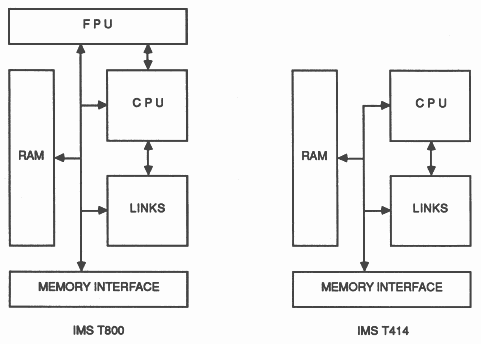
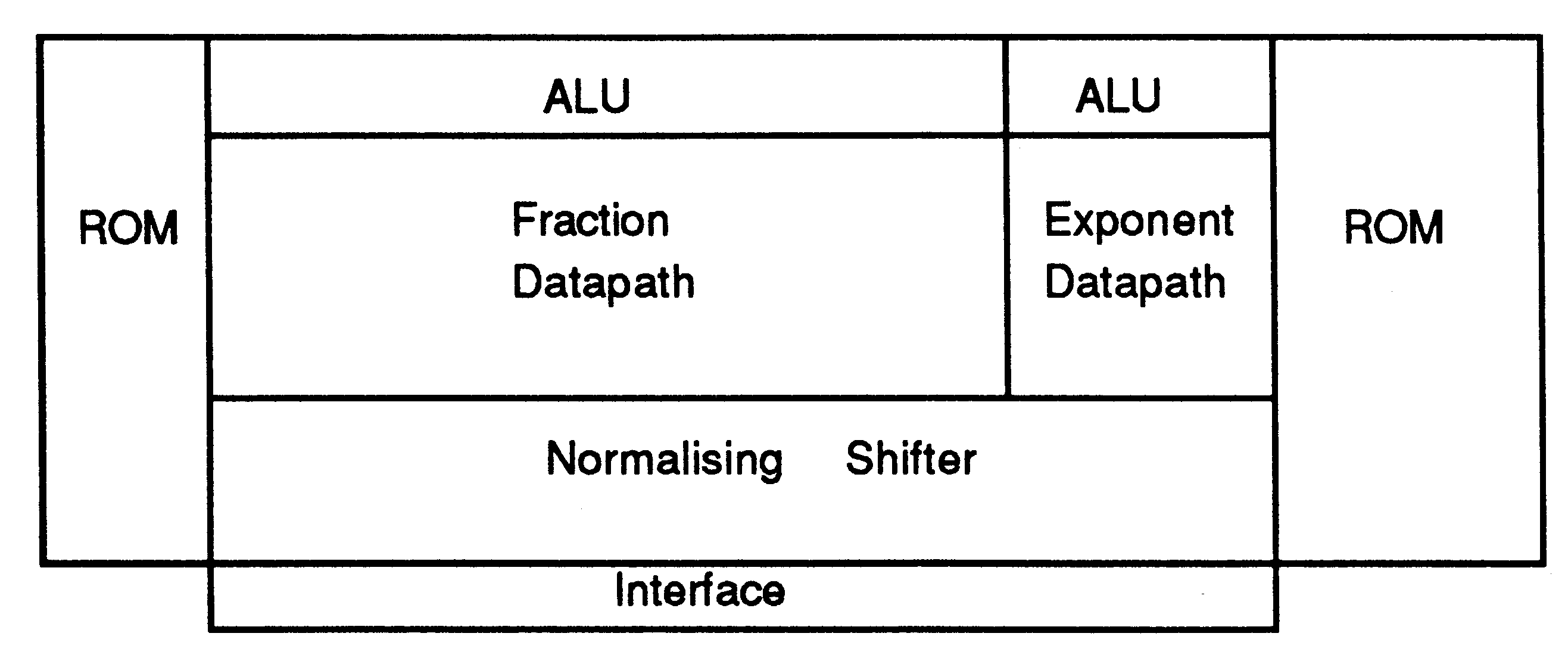
The architecture of the IMS T800 is similar to that of the IMS T414. However, in addition to the memory, links, central processing unit (CPU), and external memory interface, there is a micro-coded floating point unit (FPU) which operates concurrently with and under the control of the CPU. The block diagrams below indicate the way in which the major blocks of the IMS T800 and IMS T414 are interconnected.
The CPU of the IMS T800, just like that of the IMS T414, contains three registers (A, B and C) used for integer and address arithmetic, which form a hardware stack. Loading a value into the stack pushes B into C, and A into B, before loading A. Storing a value from A pops B into A and C into B. In addition there is an O register which is used in the formation of instruction operands. Similarly, the FPU includes a three register floating-point evaluation stack, containing the AF, BF, and CF registers. When values are loaded onto, or stored from the stack the AF, BF and CF registers push and pop in the same way as the A, B and C registers.
The addresses of floating point values are formed on the CPU stack, and values are transferred between the addressed memory locations and the FPU stack under the control of the CPU. As the CPU stack is used only to hold the addresses of floating point values, the wordlength of the CPU is independent of that of the FPU. Consequently, it would be possible to use the same FPU together with, for example, a 16 bit CPU such as that used on the IMS T212 transputer.
The IMS T800, like the IMS T414, operates at two priority levels. The FPU register stack is duplicated so that when the IMS T800 switches from low to high priority none of the state in the floating point unit is written to memory. This results in a worst-case interrupt response of only 2.5 μS (-30), or 3.7 μS (-20). Furthermore, the duplication of the register stack enables floating point arithmetic to be used in an interrupt routine without any performance penalty.
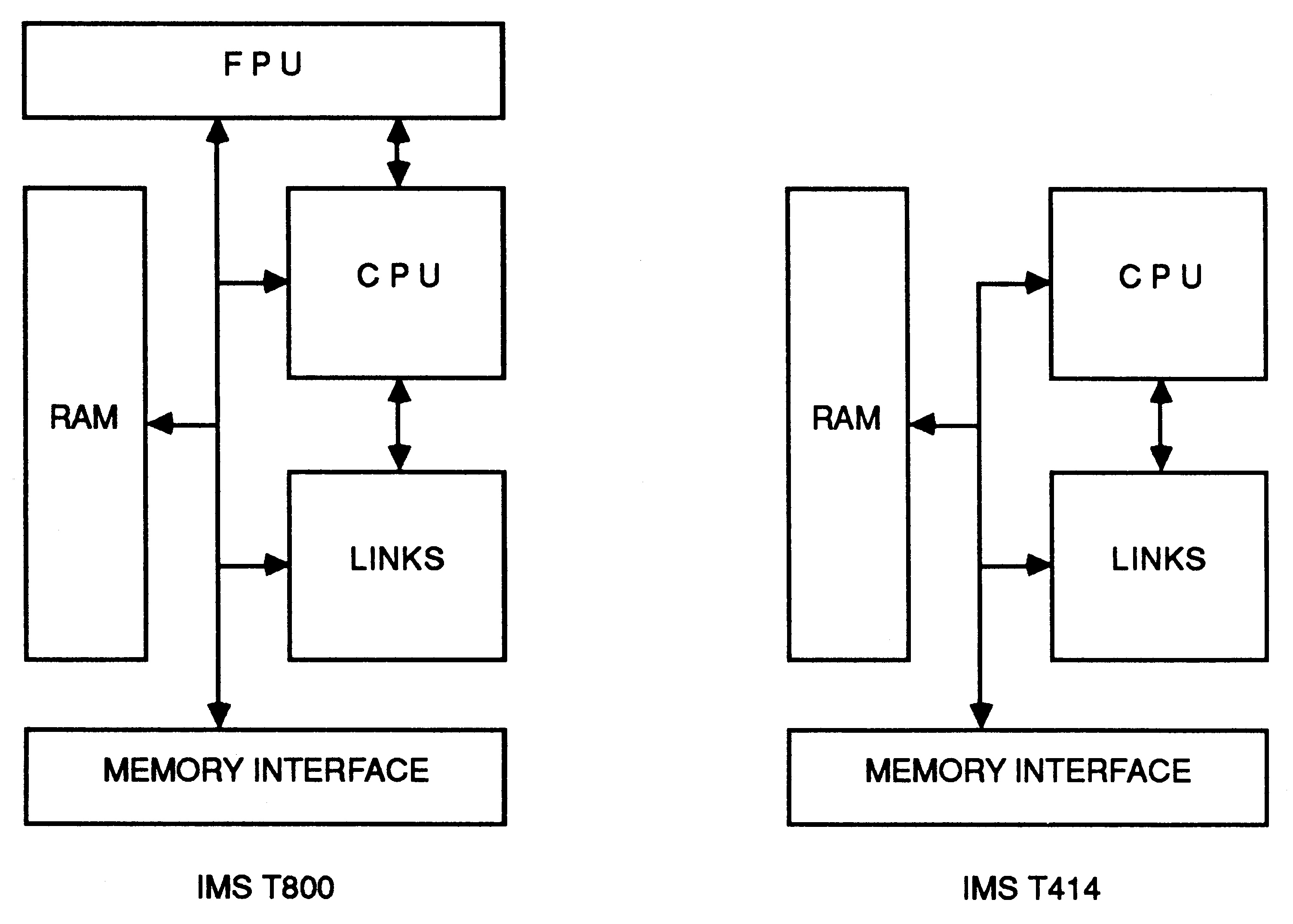
All transputers share the same basic instruction set. It contains a small number of instructions, all with the same format, chosen to give a compact representation of the operations most frequently occuring in programs. Each instruction consists of a single byte divided into two four bit parts.
The four most significant bits are a function code, and the four least significant bits are a data value. The sixteen functions include loads, stores, jumps and calls and enable the most common instructions to be represented in a single byte. As this encoding permits only 4 bits of operand per instruction two of the function codes (prefix and negative prefix) are used to allow the data part of any instruction to be extended in length. Another of the sixteen functions (operate) treats its data portion as an operation on values held in the processor registers. This allows up to 16 such operations to be encoded in a single byte instruction.
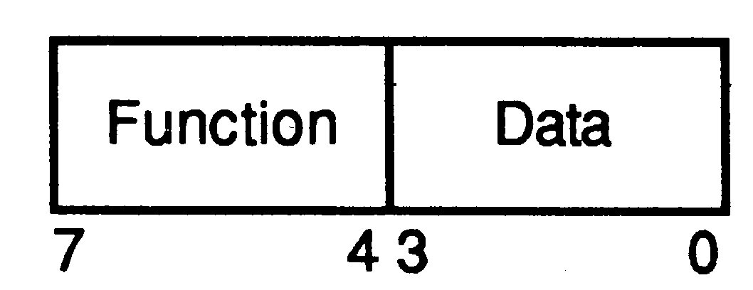
All instructions are executed by loading the four data bits into the least significant four bits of the O register, which is then used as the the instruction’s operand. All instructions except the prefix instructions end by clearing the O register, ready for the next instruction.
The prefix instruction loads its four data bits into the O register, and then shifts the O register up four places. The negative prefix instruction is similar, except that it complements the operand register before shifting it up. Consequently operands can be extended to any length up to the length of the operand register by a sequence of prefix instructions.
The prefix functions can be used to extend the operand of an operate instruction just like any other. The instruction representation therefore provides for an indefinite number of operations. The encoding of operations is chosen so that the most common operations, such as add and greater than, are represented without a prefix instruction.
The IMS T800 has additional instructions which load into, operate on, and store from, the floating point register stack. It also contains new instructions which support colour graphics, pattern recognition and the implementation of error correcting codes. These instructions have been added whilst retaining the existing IMS T414 instruction set. This has been possible because of the extensible instruction encoding used in transputers.
The core of the floating point instruction set was established fairly early in the design of the IMS T800. This core includes simple load, store and arithmetic instructions. Examination of statistics derived from FORTRAN programs suggested that the addition of some more complex instructions would improve performance and code density. Proposed changes to the instruction set were assessed by examining their effect on a number of numerical programs. For each proposed instruction set, a compiler was constructed, the programs compiled with it, and the resulting code then run on a simulator. The resulting instruction set is now described.
In the IMS T800 operands are transferred between the transputer’s memory and the floating point evaluation stack by means of floating point load and store instructions. There are two groups of such instructions, one for single length numbers, one for double length. In the description of the load and store instructions which follow only the double length instructions are described. However, there are single length instructions which correspond with each of the double length instructions.
The address of a floating point operand is computed on the CPU’s stack and the operand is then loaded, from the addressed memory location, onto the FPU’s stack. Twc new addressing operations have been added to the CPU to improve access to double-word (64-bit real and integer) values. The first of these, word subscript double, is used to index double-word values. The second of these, duplicate, is used when the CPU has to manipulate the addresses of both the more significant and less significant words of a double word object.
Operands in the floating point stack are tagged with their length. The operand’s tag will be set when the operand is loaded or is computed. The tags allow the number of instructions needed for floating point operations to be reduced; there is no need, for example, to have both floating add single and floating add double instructions; a single floating add will suffice.
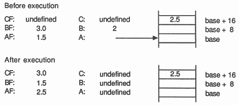
There are two instructions to load double length floating point numbers into the floating point evaluation stack from the transputer’s memory. These are floating load non-local double and floating load indexed double. The floating load non-local double instruction loads the value pointed to by the A register of the CPU’s stack. The floating load indexed double instruction has the same effect as the instruction word subscript double followed by floating load non-local double. The value in the B register is used as a double-word offset from the base pointer in the A register and the selected double length value is loaded into the AF register. The diagram below shows the effect of executing a floating load indexed double instruction.
The effect of the floating load indexed instructions can be achieved by a sequence of just two instructions. However, their presence does decrease code size; the floating load indexed double instruction is encoded in only two bytes, whereas the equivalent instruction sequence would require four bytes. This appears to be a worthwhile optimisation as this instruction sequence would be compiled for every array access.
However, there are just two floating store instructions, floating store non-local single and floating store nonlocal double. These both store the value in the AF register into the location pointed to by the A register. There are no floating store indexed instructions. This may be surprising given that the floating load indexed instructions exist; however, in any program there are less store operations than load operations and, therefore, there is less to be gained by optimising store (write to memory) operations than optimising load (read from memory) operations.
The common floating point operations of addition, subtraction, multiplication and division are provided by single instructions. These instructions operate on values in the AF and BF registers, storing the result of the operation into the AF register and popping the CF register into the BF register. Similarly, the floating point comparison operations, floating point greater than and floating point equality, compare values stored in the AF and BF registers; however, they load the result of the comparison into the A register of the CPU.
As an example, consider the following fragment of occam which sets a boolean variable converged to indicate whether the value of the 32-bit floating point variable absolute.error is less than the value of the variable epsilon.
BOOL converged:
REAL32 absolute.error, epsilon SEQ ... converged := absolute.error < epsilon ... |
The compiled code for this fragment would be:
load local pointer epsilon address of epsilon
floating load non-local single load value into FPU load local pointer absolute.error address of absolute. error floating load non-local single load value into FPU floating greater than result pushed onto CPU stack store local converged store in converged |
There are four instructions which combine loading and operating. These exist, as do the load indexed instructions, to improve code compactness. The effect of the floating load and add single instruction is just the same as the sequence floating load non-local single followed by floating add. The remaining instructions complete the set needed to load and add or multiply single and double length values. The choice of optimising only addition and multiplication in this way reflects the high usage of these operators in programs.
The depth of the register stacks in the CPU and FPU is carefully chosen. Floating point expressions commonly have embedded address calculations, as the operands of floating point operators are often elements of one dimensional or two dimensional arrays. The CPU stack is deep enough to allow most integer calculations and address calculations to be performed within it. Similarly, the depth of the FPU stack allows most floating point expressions to be evaluated within it, employing the CPU stack to form addresses for the operands.
No hardware is used to deal with stack overflow. A compiler can easily examine expressions and introduce temporary variables in memory to avoid stack overflow. The number of such temporary variables can be minimised by careful choice of the evaluation order; an algorithm to perform this optimisation is given in [Inmos ’87]. The algorithm, already used to optimise the use of the integer stack of the IMS T414, is also used for the main CPU of the IMS T800.
In the IMS T800 the FPU operates concurrently with the CPU. This means that it is possible to perform an address calculation in the CPU whilst the FPU performs a floating point calculation. This can lead to significant performance improvements in real applications which access arrays heavily. This aspect of the IMS T800’s performance was carefully assessed, partly through examination of the ’Livermore Loops’ (see appendix and [McMahan]). These are a collection of small kernels designed to represent the types of calculation performed on super-computers. They are of interest because they contain constructs which occur in real programs which are not represented in such programs as the Whetstone benchmark (see below). In particular, they contain accesses to two and three-dimensional arrays, operations where the concurrency within the IMS T800 is used to good effect. In some cases the compiler is able to choose the order of performing address calculations so as to maximise overlapping; this involves a modification of the algorithm mentioned earlier.
As a simple example of overlapping consider the implementation of Livermore Loop 7 (see appendix). The IMS T800-30 achieves a speed of 2.25 Mflops on this benchmark; for comparison the IMS T800-20 achieves 1.5 Mflops, the T414-20 achieves 0.09 Mflops and a VAX 11/780 (with fpa) achieves 0.54 Mflops. The occam program for loop 7 is as follows:
-- LIVERMORE LOOP 7
SEQ k = 0 FOR n x[k] := u[k] + ((( r*(z[k] + (r*y[k]))) + (t*((u[k+3] + (r*(u[k+2] + (r*u[k+1]))))))) + (t*((u[k+6] + (r*(u[k+5] + (r*u[k+4]))))))) |
The following explains how this program fragment is executed on the IMS T800. The explanation assumes that the floating point variable r and the floating point arrays (x, y, z, and u) are located in a global data area and must be accessed via a a static link, but that the loop count k, is in the process workspace. A compiler will generate code which first evaluates the subexpression z[k] + (r*y [k]).
The first stage in the computation of this is to load the value y[k]. The code to do this is:
load local k
load local static.link load non-local pointer y floating load indexed single |
The first load pushes the subscript k onto the CPU stack. The next load pushes the static link onto the CPU stack; the static link will contain a pointer to the base of the area of memory which contains the floating point variables and arrays. The load non-local pointer instruction generates a pointer to the yth element of that area of memory; this will be the base of the array y. The CPU stack now has its A register containing a pointer to the base of the array y, and its B register containing the subscript, k. The floating load indexed single instruction pushes the single length floating point number stored in y[k] onto the FPU stack.
The next segment of code pushes the value r onto the floating point stack and multiplies the number r in AF by y[k] in BF.
load local static.link
load non-local pointer r floating load and multiply single |
Although the floating point multiplication takes several cycles to complete, the CPU is able to continue executing instructions whilst the FPU performs the multiplication. Thus the whole of the next segment of code can be executed whilst the multiplication is being performed.
load local k
load local static.link load non-local pointer z word subscript |
This code is similar to the first section of code illustrated above. However, it explicitly executes a word subscript to compute the address of z[k]; this allows the code following to use a floating load and add single instruction which saves 2 bytes of code.
Finally, the value z[k] is pushed onto the floating point stack and added to the previously computed subexpression r*y[k]. It is not until the value z[k] is loaded that the CPU needs to synchronise with the FPU.
The computation of the remainder of the expression proceeds in the same way, and the FPU never has to wait for the CPU to perform an address calculation.
The overlapping of address calculation with floating point computation is effective even when access is being made to multi-dimensional arrays. The IMS T800 retains the fast multiplication instruction (produce of the IMS T414 which is used for the multiplication implicit in multi-dimensional array access. This instruction executes in a time dependent on the highest bit set in its second operand.
For example, in the execution of the following fragment of occam
[20][20]REAL32 A:
SEQ ... B := A[I,J] + (C / D) ... |
loading the element A[I,J] involves computing the offset of the element from the base of the array A. The transputer compiler would generate the following code for this computation
load local I load I onto CPU stack
load constant 20 load 20 onto CPU stack product multiply I by 20 load local J load J onto CPU add add J to I * 20 |
In this case the product instruction will execute in only 8 cycles (267 nS (-30), or 400 nS (-20)) and the whole address calculation will take 19 cycles which would be overlapped with the execution of the division C / D. Effectively, the overlapping allows the array accessing to be performed in only one cycle.
In designing a concurrent systems component such as the IMS T800, it is important to maximise the performance obtained from a given area of silicon; many components can be used together to deliver more performance. This contrasts with the design of a conventional co-processor where the aim is to maximise the performance of a single processor by the use of a large area of silicon. (Interestingly, however, the IMS T800-20 achieves similar performance to the 80386 with its Weitek 1167 co-processor chip set). As a result, in designing the IMS T800, the performance benefits of silicon hungry devices such as barrel shifters and flash multipliers were carefully examined.
A flash multiplier is too large to fit on chip together with the processor, and would therefore necessitate the use of a separate co-processor chip. The introduction of a co-processor interface to a separate chip slows down the rate at which operands can be transferred to and from the floating point unit. Higher performance can, therefore, be obtained from a slow multiplier on the same chip as the processor than from a fast one on a separate chip. This leads to an important conclusion: a separate co-processor chip is not appropriate for scalar floating point arithmetic. A separate co-processor would be effective where a large amount of work can be handed to the co-processor by transferring a small amount of information; for example a vector co-processor would require only the addresses of its vector operands to be transferred via the co-processor interface.
It turns out that a flash multiplier also operates much more quickly than is necessary. Only a pipelined vector processor can deliver operands at a rate consistent with the use of such devices. In fact, any useful floating point calculation involves more operand accesses than operations. As an example consider the assignment y[i] := y[i] + (t * x[i]) which constitutes the core of the LINPACK floating point benchmark. To perform this it is necessary to load three operands, perform two operations and to store a result. If we assume that it takes twice as long to perform a floating point operation as to load or store a floating point number then the execution time of this example would be evenly split between operand access time and operation time. This means that there would be at most a factor of two available in performance improvement from the use of an infinitely fast floating point unit!
Unlike a flash multiplier, a fast normalising shifter is important for fast floating point operation. When implementing IEEE arithmetic it may be necessary to perform a long shift on every floating point operation and unless a fast shifter is incorporated into the floating point unit the maximum operation time can become very long. Fortunately, unlike a flash multiplier, it is possible to design, a fast shifter in a reasonable area of silicon. The shifter used in the IMS T800 is designed to perform a shift in a single cycle and to normalise in two cycles.
Consequently, the floating point until of the IMS T800 contains a fast normalising shifter but not a flash multiplier. However there is a certain amount of logic devoted to multiplication and division. Multiplication is performed three-bits per cycle, and division is performed two-bits per cycle. This gives rise to a single length multiplication time of 13 cycles (367 nS (-30), or 550 nS (-20)) and a double length divide time of 34 cycles (1.07 μS (-30), or 1.6 μS (-20)).
One other aspect of floating point arithmetic which was carefully examined was the implementation of standard scientific functions (sqrt, sin, etc). Trigonometric functions are generally implemented by algorithms which make use of an approximation which is only accurate over a small part of the function’s domain. This is possible because mathematical identities enable the full function to be computed from the partial approximation. Algorithms differ in the way in which they compute the approximation; two methods of computing the approximation were considered during the design of the IMS T800.
The first method is called CORDIC which was developed for hardware implementation and is used in some floating point co-processor chips such as the i8087. This requires the addition of significant quantities of hardware into the datapath and the storage of large look-up tables. Even with this hardware the best performance which could be achieved would be to generate one bit of result every four cycles, resulting in a minimum evaluation time for the reduced function of about 230 cycles (double length).
The second method is polynomial approximation. This requires no additional hardware in the FPU. The evaluation time will vary from function to function, but for the sin function only about twice the number of cycles required by CORDIC would be used since the implementation of multiplication generates three bits of product every one cycle.
In practice we are interested in the evaluation time for the function proper, not just the reduced function. Once the time for argument reduction and function generation have been added to the time for the evaluation of the partial function it is dear that there is no possibility of a CORDIC based implementation being even twice as fast as polynomial based implementation. For this reason the IMS T800 contains no special support for trigonometric function evaluation.
This comparison can also be extended to show that if a processor with even faster trigonometric function evaluation were required it should be achieved by increasing the speed of the processor’s multiplication. This would have the additional benefit that it would increase performance on virtually all applications, not just those which make heavy use of trigonometric functions.
The situation is rather different with regard to the square root function. Here the IEEE standard requires that the result is produced correct to the last bit and this is not easy to achieve by simple polynomial evaluation. Furthermore it only requires a small amount of additional hardware to perform square root in hardware and this has been done in the IMS T800.
The block diagram below illustrates the physical layout of the floating point unit.
The datapaths contain registers and shift paths. The fraction datapath is 59 bits wide, and the exponent data path is 13 bits wide. The normalising shifter interfaces to both the fraction data path and the exponent datapath. This is because the data to be shifted will come from the fraction datapath whilst the magnitude of the shift is associated with the exponent datapath. One further interesting aspect of the design is the micro-code ROM. Although the diagram shows two ROMs, they are both part of the same logical ROM. This has been split in two so that control signals do not need to be bussed through the datapaths.
The IMS T414 has microcode support for 32-bit floating point arithmetic which gives it performance comparable with the current generation of floating point co-processors. It achieves an operation time of about 10 microseconds on single length IEEE 754 floating point numbers. The IMS T800-20 betters the floating point operation speed of the IMS T414 by more than an order of magnitude; its operation times are shown below
| IMS T800-30 | IMS T800-20 | IMS T414-20
| ||||
| single | double | single | double | single | double | |
| operation | ||||||
| add | 233ns | 233ns | 350ns | 350ns | 11.5μs | 28.3μs |
| subtract | 233ns | 233ns | 350ns | 350ns | 11.5μs | 28.3μs |
| multiply | 367ns | 667ns | 550ns | 1000ns | 10.0μs | 38.0μs |
| divide | 567ns | 1067ns | 850ns | 1600ns | 12.3μs | 55.8μs |
The operation time is not a reliable measure of performance on real numerical programs. For this reason, floating point performance is often measured by the Whetstone benchmark. The Whetstone benchmark provides a good mix of floating point operations, and also includes procedure calls, array indexing and transcendental functions. It is, in some sense, a ’typical’ scientific program.
The performance of the IMS T414 and IMS T800 compared with other processors as measured by the Whetstone benchmark is shown below:
| Processor | Whetstones/second
| |
| single length
| ||
| Intel 80286/80287 | 8 MHz | 300K |
| IMS T414-20 | 20 MHz | 663K |
| NS 32332-32081 | 15 MHz | 728K |
| MC 68020/68881 | 16/12 MHz SUN 3 | 755K |
| VAX 11/780 FPA | UNIX 4.3 BSD | 1083K |
| IMS T800-20 | 20 MHz | 4000K |
| IMS T800-30 | 30 MHz | 6000K |
This table shows that although the IMS T414 has an operation time three times slower than the MC68881 co-processor it performs only 25% worse than the MC68020 + MC68881 co-processor (as measured by the Whetstone benchmark). This is because the speed of evaluating a floating point expression depends on two factors; the speed at which operands are transferred to and from the floating point unit and the speed of the unit itself. By careful balancing of these the single chip IMS T800-20 achieves more than five times the Whetstone performance of the MC68020/MC68881 combination.
Another important measure is the performance obtained from a given area of silicon. For example, four IMS T800-30 chips occupy an area similar to the i80386 together with the Weitek 1167 chip set, and on single length floating point will deliver 6 times the performance in any concurrent application. In terms of circuit board area, the effect is even more dramatic; the IMS T800 requires negligible support circuitry and can even be used without external memory.
One of the concerns of engineers designing microprocessors into life-critical systems is the correctness of the implementation of those microprocessors. The complexity of a floating point unit is such that It is impossible to validate by exhaustive testing. The approach which INMOS has taken is to make use of the most advanced formal methods to ensure the correct implementation of the IEEE 754 standard for floating point arithmetic. This work has been undertaken in co-operation with the Programming Research Group at Oxford University and has made use of the formal semantics of the occam programming language. Inmos has found that the use of formal methods in complex designs greatly decreases design time as well as ensuring correctness.
The specification language Z (see appendix) was used extensively during the design of the IMS T800, both to express the IEEE 754 standard mathematically and to specify instructions precisely. The first stage of implementation was to write a software package in the occam language and to prove that it met the specification. (This package is used to provide floating point arithmetic for various occam implementations, including that for the IMS T414). Using an interactive program transformation system, the occam package was then transformed into the microcode for the IMS T800.
This design process is illustrated using one instruction from the sequence of instructions executed by the IMS T800 to perform floating point to integer conversions. This instruction occurs in the middle of the sequence, after the floating point number has been rounded into an integer in floating point format. The instruction checks that the rounded value lies within the range of numbers representable as an integer and, if not, sets the error flag.
The precise specification of range checking is expressed in Z as:
Floating_Check-Integer-Range
Areg, Areg’ : Floating-Point-Register Error_Flag, Error_Flag’ : bool fv Z Areg’ = Areg fv Areg [MinInt,MaxInt] => Error_Flag’ = Error_Flag fv Areg [MinInt,MaxInt] => Error_Flag’ = true |
In this specification the primed variables Areg’ and Error_Flag’ denote the values of registers after the operation, and the unprimed variables denote the values before. Maxint and Minint are constants defined by the integer format and fv is a function that returns the value of a floating point register. The predicates state that the operation is only defined when Areg contains an ”integer” value, that Areg is unchanged by the operation and that Error_Flag is set if Areg lies outside the storable integer range and is unchanged otherwise.
The high level occam implementation is as shown below. Its correctness depends on proving two assertions. Firstly, that there is an exponent, LargestINTExp, such that every floating point register with a smaller exponent lies in [Minlnt,Maxlnt], and secondly, that a register with a negative sign bit, an exponent equal to LargestINTExp and a fraction with only the implied msb set, has an fV of Minint.
IF
Areg.Exp < LargestINTExp SKIP (Areg.Sign = NEGATIVE) AND (Areg.Exp = LargestINTExp) AND (Areg.Frac = MSBit) SKIP TRUE SetError (ErrorFlag) |
In the above code, the occam variable Areg.Exp is used to represent the contents of the exponential part of the FA register of the FPU. Similarly, Areg. Sign and Areg.Frac represent the sign-bit and fraction part. This code first checks to see if the exponent is smaller than LargestINTExp; if it is then the value in the FA register is in range and no further action is to be performed. Otherwise, the code checks if the value in the FA register has a negative sign bit, an exponent equal to LargestINTExp and a fraction with only the most significant bit set; if it does then, again, no further action is performed. Otherwise, the value in the FA register is out of range and the error flag is set.
The program above can be transformed using the laws of occam. First the condition on Areg. Sign is pulled to the outside. Then the program is transformed into processes and variables defined in terms of operations found in the floating point microcode. This involves the use of register and bus operations to perform the comparisons together with explicit tests of the resulting flags. At this stage the processes are also grouped into the sequences of operations that form each micro-instruction. For brevity the negative case is omitted in this illustration:
SEQ
AregSignNEGATIVE := (Areg.Sign = NEGATIVE) ExpZbus := (Areg.Exp - LargestINTExp) ExpZbusNeg := ExpZbus < 0 IF AregSignNEGATIVE ... negative case NOT AregSignNEGATIVE IF ExpZbusNeg SKIP NOT ExpZbusNeg SetError(ErrorFlag) |
The low level occam implementation is then transformed into a ”flattened” form that makes explicit use of a micro-instruction pointer. This form uses a WHILE loop and explicit testing of the next instruction register (NextInst) to simulate the sequencing of the micro-code. If the resulting micro-code involves no loops it is possible to transform it back into the original form mechanically. In the program below the SetError (ErrorFlag) process has been moved into a separate micro-instruction, OutOfRange.
INT NextInst :
SEQ NextInst := FloatingPointCheckIntegerRange WHILE NextInst <> NOWHERE IF NextInst = FloatingPointCheckLntegerRange SEQ AregSignNEGATIVE := (Areg.Sign = NEGATIVE) ExpZbus := (Areg.Exp - LargestINTExp) ExpZbusNeg := ExpZbus < 0 IF AregSignNEGATIVE ... negative case NOT AregSignNEGATIVE IF ExpZbusNeg NextInst := NOWHERE NOT ExpZbusNeg NextInst := OutofRange NextInst = OutofRange SEQ SetError(ErrorFlag) NextInst := NOWHERE ... negative case micro instructions |
The flattened occam code is then transformed into micro-code assembler. This is done by a pattern matching and textual substitution program. Without the use of mechanical assistance this is a very laborious and error-prone task. The program below shows the micro-code which results from translating the FloatingPointCheckIntegerRange micro-instruction of the previous example.
FloatingPointCheckIntegerRange:
ConstantLargestINTExp ExpXbusFromAreg ExpYbusFromConstant ExpZbusFromXbusMinusYbus GOTO Cond1FromAregSign -> (Cond0FromExpZbusNeg -> (... , ...), Cond0FromExpZbusNeg -> (NOWHERE,OutofRange)) |
The use of the high-level specification language Z provides short and precise specifications of instructions, and, being mathematically based, avoids the problems of interpreting natural language specifications. This specification can be implemented fairly naturally, at a high level, in occam. This implementation can be proved correct, using occam’s denotational semantics. The algebraic semantics of occam then allow the occam to be transformed into a form that corresponds to the micro-code.
Z specification
| 1 V high level occam | 2 V low level occam "tree code" | 3 V low level occam "flat code" | 4 V micro-code |
Each of steps 1 to 3 can be proven correct using the formal semantics of occam. The translation and compilation of step 4 could also be proved correct. In practice, both steps 1 and 2 were performed backwards; that is, an implementation was written and then transformed back into the previous specification. This process made use of an occam source transformation system, written in ML and implemented by the Programming Research Group at Oxford University. Steps 3 and 4 are performed semi-mechanically by programs. Although these have not been formally proved, their use is more reliable than doing the same work by hand; computers do not mistakenly miss out lines of micro-code due to boredom!
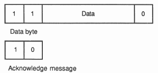
A link between two transputers is implemented by connecting a link interface on one transputer to a link interface on the other transputer by two one-directional signal wires, along which data is transmitted serially. The two wires provide two occam channels, one in each direction. This requires a simple protocol to multiplex data and control information. Messages are transmitted as a sequence of bytes, each of which must be acknowledged before the next is transmitted. A byte of data is transmitted as a start bit followed by a one bit followed by eight bits of data followed by a stop bit. An acknowledgement is transmitted as a start bit followed by a stop bit. An acknowledgement indicates both that a process was able to receive the data byte and that it is able to buffer another byte.
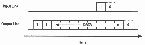
The protocol permits an acknowledgement to be generated as soon as the receiver has identified a data packet. In this way the acknowledgement can be received by the transmitter before all of the data packet has been transmitted and the transmitter can transmit the next data packet immediately. The IMS T414 transputer does not implement this overlapping and achieves a data rate of 0.8 Mbytes per second using a link to transfer data in one direction. However, by implementing the overlapping and including sufficient buffering in the link hardware, the IMS T800 more than doubles this data rate to 1.8 Mbytes per second in one direction, and achieves 2.4 Mbytes per second when the link carries data in both directions. The diagram below shows the signals that would be observed on the two link wires when a data packet is overlapped with an acknowledgement.
The ”bit-blt” operations of a conventional graphics processor no longer seem appropriate in these days of byte (or greater) per pixel colour displays. The fast block move of the IMS T414 make it suitable for use in graphics applications using byte-per-pixel colour displays. Indeed, the IMS B007 colour graphics evaluation board uses it in such a manner.
The block move on the IMS T414 is designed to saturate the memory bandwidth, moving any number of bytes from any byte boundary in memory to any other byte boundary using the smallest possible number of word read and write operations. Using the transputer’s internal memory the block move sustains a transfer rate of 60 Mbytes per second (-30), or 40 Mbytes per second (-20); using the fastest possible external memory the block move sustains 20 Mbytes per second (-30) or 13.3 Mbytes per second (-20).
The IMS T800 extends this capability by incorporation of a two-dimensional version of the block move which can move windows around a screen at full memory bandwidth, and conditional versions of the same block move which can be used to place templates and text into windows. One of these operations copies bytes from source to destination, writing only non-zero bytes to the destination. A new object of any shape can therefore be drawn on top of the current image. All of these instructions achieve the speed of the simple IMS T414 move instruction, enabling a 1 million pixel screen to be drawn 13 times per second.
The three new instructions are concerned with moving a two-dimensional block of data from source to destination. The instructions differ in how the source is used to modify the destination. Unlike the conventional ”bit-bit” instruction, it is never necessary to read the destination data.
The instructions are described in occam:
PROC Move2d ([][]BYTE Source, sx, sy,
[][]BYTE Dest, dx, dy, width, length) SEQ y = 0 FOR length [Dest[y+dy] FROM dx FOR width] := [Source[y+sy] FROM sx FOR width] |
This moves a block of size width x length which starts at byte Source [By] [sx] to the block starting at byte Dest[dy][dx].
PROC Draw2d ([][]BYTE Source, sx, sy,
[][]BYTE Dest, dx, dy, width, length) BYTE temp: SEQ line = 0 FOR length SEQ point = 0 FOR width SEQ temp := Source[line+sy][point+sx] IF temp = 0(BYTE) SKIP TRUE Dest[line+dy][point+dx] := temp |
This moves a block of size width x length which starts at byte Source[sy][sx] to the block starting at byte Dest[dy][dx]. However for every byte transferred a check is made to see if it is zero. If this is the case then the byte is not copied, and the destination remains unaltered.
PROC Clip2d ([][]BYTE Source, sx, sy,
[][]BYTE Dest, dx, dy, width, length) BYTE temp: SEQ line = 0 FOR length SEQ point = 0 FOR width SEQ temp := Source[line+sy][point+sx] IF temp = 0(BYTE) Dest[line+dy][point+dx] := temp TRUE SKIP |
This moves a block of size width x length which starts at byte Source[sy][sx] to the block starting at byte Dest[dy][dx]. However for every byte transferred a check is made to see if it is zero. If this is the case then that byte is copied.
Draw2d and Clip2d are complementary and are used for the copying of irregular shapes onto the screen and the creation of templates.
Like the transputer’s one dimensional block move, the Move2d, Draw2d and Clip2d instructions move data from any byte address in memory to any byte address using the smallest possible number of single word transfers. When executing a Draw2d operation, data is written in whole words, and hardware is used to suppress the generation of individual byte write signals corresponding to zero bytes in the source. Further, the write cycle is omitted completely if all bytes in the source word are found to be zero. Clip2d is similarly implemented using the smallest number of word read and write operations. Consequently, Draw2d and Clip2d normally operate faster than simple moves.
Move2d, Draw2d and Clip2d are not restricted to operations on single byte pixels. For example, 3 byte (24 bit) pixels can be treated in exactly the same way as single byte pixels, with a zero pixel being represented by three zero bytes, and non-zero pixels being represented by three non-zero pixels. Pixels less than a byte can be implemented by omitting unnecessary bit planes from the video memory. By regarding an image as a 2 dimensional array of pixels, each of which is itself an array of bytes, it is possible to use the same graphics software on systems with differing pixel sizes.
Drawing proportional spaced text provides a simple example of the use of the IMS T800 instructions. The font is stored in a two dimensional array Font; the height of Font is the fixed character height, and the start of each character is defined by an array start. The textures of the character and its background are selected from an array of textures; the textures providing a range of colours or even stripes and tartans!
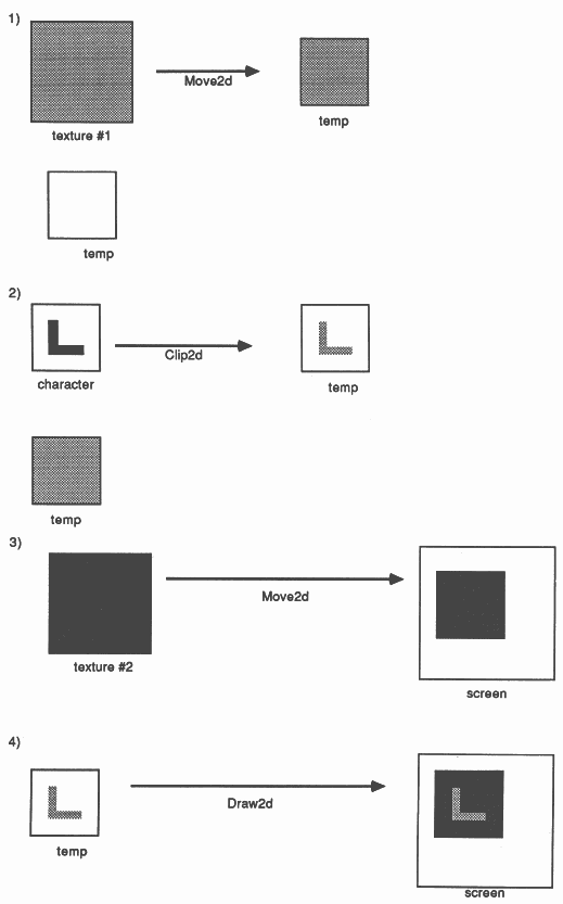
An occam procedure to perform such drawing is given below and the effect of each stage in the drawing process is illustrated by the diagrams on the final page of this document. First, (1) the texture for the character is selected and copied to a temporary area and (2) the character in the font is used to clip this texture to the appropriate shape. Then (3) the background texture is selected and copied to the screen, and (4) the new character drawn on top of it.
-- Draw character ch in texture F on background texture B
PROC DrawChar(VAL INT Ch, F, B) SEQ IF (x + width[ch]) > screenwidth SEQ x := 0 y = y + height (x + width[ch]) <= screenwidth SKIP [height][maxwidth]BYTE Temp : SEQ Move2d(Texture[F], 0, 0, Temp, 0, 0, width[ch], height) Clip2d(Font[ch], start[ch], 0, Temp, 0, 0, width[ch], height) Move2d(Texture[B], 0, 0, Screen, x, y, width[ch], height) Draw2d(Temp, 0, 0, Screen, x, y, width[ch], height) x := x + width[ch] |
This procedure will fill a 1 million pixel screen with proportionally spaced characters in about 1/6 second. Obviously, a simpler and faster version could be used if the character colour or background colour was restricted. The operation of this procedure is illustrated on the next page.
The IMS T800 floating point transputer provides a very high performance building block for concurrent systems. The design of the IMS T800 demonstrates that it is not desirable to use co-processors to achieve high performance floating point capability. The careful consideration of silicon economics has enabled the IMS T800 to incorporate a floating point unit, a central processing unit, memory and a communication system in a single device; it is a complete scientific computer on a single chip. For example, the 4 kbytes of onchip memory allows the IMS T800 to be used, without external memory, in a number of signal processing applications. The fact that the floating-point performance of the IMS T800 exceeds its fixed-point performance on multiply-accumulates removes the need to design algorithms which use fixed-point arithmetic.
The IMS T800 forms the basis of the most powerful supercomputer in Europe, currently under construction at Edinburgh University. This will contain 1,000 transputers operating on one giga-byte of main store and should be operational by April 1988. Whilst this may seem to be a very large machine, the continuing improvement in VLSI technology means that such a machine will occupy only a few cubic feet in the early 1990s. Even today, using conventional packaging and printed circuit board technology, machines built from the IMS T800-20 can achieve a ”performance density” of 1.5 Gflop per cubic foot.
Harp ”Phase 1 of the development and application of a low cost, high performance multiprocessor machine”, J G Harp et al, pp 551-562, ESPRIT ’86: Results and Achievements, Elsevier Science Publishers B.V.
IEEE ”IEEE Standard for Binary Floating-Point Arithmetic”, ANSVIEEE Std 754-1985
Inmos ’84 ”IMS T414 reference manual”, Inmos Limited 1984
Inmos ’87 ”The transputer instruction set - a compiler writers’ guide”, Inmos Ltd
McMahon ”The Livermore Fortran Kernels: A Computer Test of the Numerical Performance Range”, Frank H. McMahon, Lawrence Livermore National Laboratory, UCRL-53745
It is not possible to give a comprehensive description of occam in the space available. However, the following overview explains the basic concepts of the language and explains those details which are required in order to understand the examples in the paper.
The occam programming language was developed to allow concurrent, distributed, systems to be programmed. The emphasis is placed on distributed because it was for this area that previous languages are unsuited. The occam language enables a system to be described as a collection of concurrent processes, which communicate with each other and with peripheral devices through channels. The concurrent processes do not communicate via shared variables, and thus occam is a suitable language for programming systems where there there is no store which is shared between processors in the system.
occam programs are built from three primitive processes: v := e assign expression e to variable v c ! e output expression e to channel c c ? v input from channel c to variable v
The primitive processes are combined to form constructs:
SEQuential components executed one after another PARallel components executed together ALTernative component first ready is executed
A construct is itself a process, and may be used as a component of another construct. The syntax of oCCam uses indentation to indicate program structure, thus the occam program below consists of two parallel processes. The first process inputs from the channel source into next.problem. The second process itself consists of two processes to be executed sequentially. The first is an instance of the procedure compute.next.solution, and the second, which is executed after the first has terminated, outputs solution onto channel result.
PAR
source ? next.problem SEQ compute.next.solution(this.problem, solution) result ! solution |
Conventional sequential programs can be expressed in occam with variables and assignments, combined in sequential constructs. IF and WHILE constructs are also provided. The IF construct test a number of conditions in sequence, when one is found to be true, the associated process is executed. The example below shows how this might be used to compare two numbers, a and b, and to record their order.
IF
a > b order := gt a < b order := lt TRUE order := eq |
Concurrent programs can be expressed with channels, inputs and outputs, which are combined in parallel and alternative constructs.
Each occam channel provides a communication path between two concurrent processes. Communication is synchronised and takes place when both the inputting process and the outputting process are ready. The data to be output is then copied from the outputting process to the inputting process, and both processes continue.
An alternative process may be ready for input from any one of a number of channels. In this case, the input is taken from the channel which is first used for output by another process.
Although the first version of occam (as described in the occam Programming Language) had only a single data type and only one dimensional arrays, the version of the language used in this paper, occam 2, supports several data types and multi-dimensional arrays. Arrays may be assigned, communicated between processes and passed as parameters to procedures. occam permits a sub-array of an array to be used as an array. For example, the following program declares a 10 element arrays of integers, a, and then, in parallel inputs to the first 5 elements of a from the channel c, and to the second 5 elements from the channel d. (Note that in occam the first element of an array is element 0).
[10] INT a :
PAR c ? [a FROM 0 FOR 5] c ? [a FROM 5 FOR 5] |
One further feature of occam which requires explanation is the replicated constructor. The examples in the paper are all of replicated SEQs which have a similar effect to a FOR loop in a conventional language. The replicated SEQ
SEQ i = base FOR count
a[i] := i |
is implemented as a loop and is equivalent to the following
SEQ
a[base] := base a[base + 1] := base + 1 ..................... a[base + count - 1] := base + count - 1 |
The Livermore Fortran Kernels [McMahon] (commonly known as the Livermore Loops) are a set of 24 computation kernels designed to measure realistic floating-point performance on FORTRAN applications. They differ from a number of other standard benchmark programs in that they do not produce a single figure of merit, but a set of figures, one for each kernel. They represent a useful source of information about the structure of scientific programs, and as such, were studied during the design of the IMS T800.
Livermore Loop 7, mentioned in this paper, is an ”equation of state” fragment. The FORTRAN code for this loop is
DO 7 k= 1,n
X(k)= U(k ) + R*( Z(k ) + R*Y(k )) + . T*( U(k+3) + R*( U(k+2) + R*U(k+1)) + . T*( U(k+6) + R*( U(k+5) + R*U(k+4)))) 7 CONTINUE |
The program in the paper is written in occam 2 and it is for this version that the code and performance figure is given. The implementation of occam and FORTRAN will differ slightly as the two languages allocate store differently.
The specification notation Z has been developed to tackle the problems of specify actual systems. Z originated with Jean-Raymond Abrial and has been developed and used extensively by members of the Programming Research Group, Oxford University.
A Z specification consists of a combination of a formal text and a natural language description. This formal text provides the precise specification while the natural language text introduces and explains the formal parts. The formal text has two parts: the schema language, which provides a means of structuring the specification, and the mathematical language, which allows for the preciseness of the specification. The mathematical language is based largely on set theory and enables an abstract mathematical view of the objects being specified to be taken. The schema language enables specifications of large systems to be broken into more manageable sections.
The combination of natural language for explanation, and the schema language produces specifications that are more readable than pure mathematics. In addition, the mathematical nature of the specifications enable implementors to use mathematical proofs to ensure the correspondence of their implementations with the specification.
The formal part of a Z specification makes use of ”schemas”. The schema consists of two ”boxes”. The top box contains the signature which introduces the variables of the specification. The lower box contains a list of predicates which constrain the values that the variables may take.
The following is an example of a Z specification:
If the reset signal is set then the Count operation sets the register to 0, otherwise it increments the register.
Count
| |
| value, value’ | : N |
| reset? | : bool |
| reset? ⇒ | value’ = 0 |
| ¬reset? ⇒ | value’ = value + 1 |
This schema, named Count, introduces 3 variables; value, value’ and reset. Conventionally, primed variables such as value’ represent values of state variables after an operation, while their unprimed counterparts represent the values before the operation. Variables with names ending in ”?”, such as reset, are conventionally inputs to an operation. The values are constrained by two predicates (conventionally these are and-ed together, unless explicitly written otherwise). These predicates formally specify the behaviour of the operation described in the informal text that precedes the schema. This schema gives a precise specification of the operation; what it has not done is to dictate how the counter is implemented (number of bits etc) as these are implementation details.