|
|
| A transputer based radio-navigation system _____________________________________________________________________ |
| INMOS 72-TCH-000 |
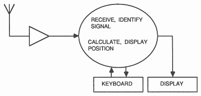
The speed and multi-processing capabilities of the transputer make it ideal for demanding signal processing, calculating and control tasks (figure 1). A navigation system needs all these facilities, and the LORAN C system, operating at 100kHz, gives the opportunity for the transputer to capture the incoming radio frequency in real time, without demodulation.
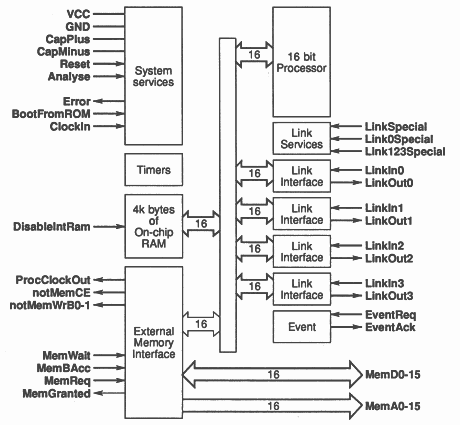
The T222 transputer is the 16-bit member of the transputer family. It has 4K bytes of 50ns static RAM on the chip, which allow it to operate at 20 MIPS (peak). The memory can be extended externally, the external interface being optimised for static memory, with separate address and data lines. Thus Static RAM or program ROM can be attached with no TTL glue logic. The T222 has four serial links operating at 5, 10 or 20 Mbaud rates, designed for connections between transputers or to peripherals such as link adapters. These links have full duplex DMA into or out of the transputer memory, giving the processor the equivalent of eight high-speed DMA controllers on chip. Also on the transputer are a hardware scheduler and timer, and all these taken with the language occam make it a very powerful general purpose processor.
The incentive to design a LORAN C system is given by the imminent opening of a new experimental chain of transmitters serving Northern Europe. The system already covers most of the world’s oceans, and also the Mediterranean, but southern Britain has lacked coverage.
LORAN (LOng-range RAdio Navigation) is a system run for ships and aircraft by the US government. Like the Decca system, it works by measuring the relative delays from several transmitters, but being long-range, it has far fewer chains, operating at much lower frequency, and no charge is made for its use.
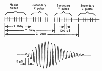
All the transmitters operate on one frequency, but they transmit at a low duty cycle with each chain having a different repetition rate. Thus the receiver can identify the valid signals as those operating at the desired rate, and although one particular signal may be blotted out by another chain, as no two chains operate at co-multiple rates, the signal can be recovered on the next frame (see figure 2).
The transputer has an inherent response time to external stimuli of between one and three micro-seconds, and has an internal resolution of one microsecond. Therefore it could theoretically resolve RF information to an accuracy of three (... (3-1)+1...) microseconds, which at the speed of light would give a navigation system an accuracy of around a kilometre. However, each result can be produced from an average of around 150 such measurements, which would improve the accuracy to around 300 metres. This is because the variable response time can be averaged out, but the resolution cannot because of the high stability of the clocks used.
The design used here improves on this accuracy by capturing the phase of the incoming signal relative to a crystal clock. The amplified filtered signal is used to clock a latch to sample a counter. In keeping with the transputer architecture, the latch used is a link adapter, which allows DMA type transfer of the data into the transputer, and the appropriate stimulus to the hardware scheduler is generated automatically. The crystal oscillator is inexpensive, as it is required for the transputer anyway, but improves the resolution from one microsecond to better than 10 nanoseconds, which makes analogue noise the predominant problem.
At 100kHz, the events must be trapped at a 10 microsecond rate, which makes the transputer’s low latency and rapid process switch time of paramount importance in this application. Any other processor attempting this task would have to hang mid-cycle awaiting the signal on a wait pin to achieve low enough latency, and thus would be unable to perform the trig operations or the system control at the same time. The closest alternative appears to be the Intel 8096, which has a latency of up to 21 microseconds, but does have timers and a fifo that would allow this to be performed only once per seven inputs. This however prevents external upgrading of the internal two-microsecond timer as shown on the transputer based design.
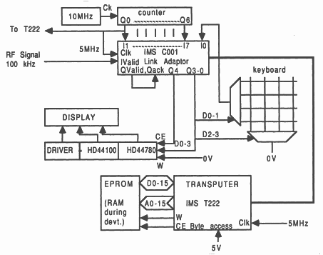
A block diagram of the system is shown in figure 3, and a circuit diagram of the digital section in figure 4.
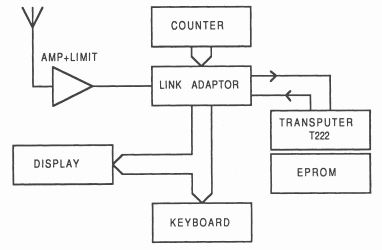
The basic elements are a high-gain narrow band amplifier to capture the incoming signal, which is only short bursts of RF, so energy-storing LC circuits are avoided where possible, a counter to measure the phase, a transputer to do signal processing and trigonometric calculation, besides controlling the system, and a keyboard and display.
The interface between the transputer and the analogue and I/O sections has been designed using the IMS Coil Link Adapter. The total input requirements are one bit from the analogue section, the carrier, seven from the counter, and one from the keyboard scanner. The carrier is not fed to the transputer, but used as me ’Input Valid’ signal to strobe the current value of the counter, i.e. the relative phase of the signal, into the link adapter input pins. The spare input, 10, is used to receive the open/closed signal from the keyboard matrix, if implemented.
The output requirements are four bits to drive the keyboard scanner, the same four being used as a data bus to the LCD display driver, and a bit to clock the display driver. This leaves three bits spare, which could be used to enlarge the keyboard matrix, or to operate LEDs or alarms for carrier fail or offtrack error.
The keyboard scanner works by taking the four bits D0-3 and decoding them in a CMOS analogue multiplexer into two one-out-of-four signals, giving a 16 key crosspoint matrix. The appropriate Y-wire is connected to ground, and the selected X-wire is fed to the 10 input of the Link Adapter, with a pull-up resistor. Thus, if the currently scanned key is depressed, the input will be a zero, if not, it will be a one. The processor must scan the keyboard, by outputting all 16 possibilities on the highway, at an appropriate interval, say 100 milliseconds. There are three further bits available on the output side of the link adapter that could be used to expand the matrix to 64 keys, which would allow a QWERTY keyboard in a more sophisticated implementation.
The display is an LCD module, available assembled complete with controller, or buildable separately. The driver is a Hitachi 44780, and this is configured to communicate in a four bit mode, so that it can be driven from a link adapter, with a fifth bit used as a timing strobe under software control.
The processing module is entirely separate from the rest, and this may be useful in improving the screening of the sensitive analogue stages from processor noise.
The IMS T222 transputer is a self contained computing engine, with RAM, CPU, timers and communications controllers all on the one chip. The only external requirements in this type of embedded system are a program ROM and a 5MHz clock.
The ROM is a standard EPROM, as fast as possible. If an EPROM is available that can keep up with the transputer (100ns cycle!), then no TTL is required, all the necessary chip enable signals are generated by the transputer. Choosing a slower speed option transputer may be worthwhile, for this reason alone, providing the faster parts of the software still operate. If higher performance is required, choose a fast option transputer and use a shift register off the transputer clock to delay memory cycles using the wait pin. If this solution is chosen, there are benefits in copying the code for the front end signal capture process into internal RAM at start-up, giving the ultimate performance.
Only one ROM chip is required, as the T222 has the ability to use 8 or 16-bit data paths externally, depending on the state of an external pin.
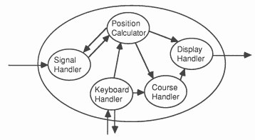
The occam language gives the programmer the ability to map his application onto a yet-to-be determined number of processors, maintaining all the potential for parallelism that exists in the underlying application. The methodology of a parallel language is very different from the sequential approach. At the highest level, all the requirements of the system can be specified as inputs and outputs to a monolithic process, and me specification of that process is the relationships of its outputs to its inputs. Thus we can draw the diagram of figure 5. However, processes are hierarchical, that is we can divide up the work of the main process into several subsidiary processes, with appropriate interconnections, and similarly specify each them individually. They do not interact in any way except by messages over the connecting channels, as there is no shared memory, so each can be separately debugged, and the decision as to which is in hardware, and which groups on which processor can be left until later. This divide-and-conquer mechanism can be repeated indefinitely, until the base processes are simple to write and thus error-free (see figure 6).
CHAN OF BYTE signal, keyin, keyout, displayout:
PLACED PAR PROCESSOR 1 T222 CHAN OF INT s.to.p, p.to.c, p.to.s, k.to.c, c.to.d, p.to.d: PLACE signal AT link0in: PLACE displayout AT link0out: PAR ... Signal handler (s) ... Position calculator (p) ... Keyboard handler (k) ... Course handler (c) ... Display handler (d) |
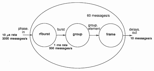
For the lowest processes, which are sequential, normal flowchart practice can be used, although with correct system design and well commented code, the programmer can go directly from the process diagram and specification to the occam source. The signal processing function divides cleanly into three processes as shown in figure 7. The first process identifies valid carrier transitions, the second valid carrier bursts, collating them into groups, and the third identifies the elements of the required frame, corresponding with the group repetition interval of the LORAN chain in use.
{{{ navsys
PROC signal.processing (CHAN OF BYTE keyboard, screen) ... proc decls ... decls PAR ... test harness rfburst (phase.in, burst) group (burst, group.element) frame (group.element, delays.out, control [chains + 1]) : }}} |
Occam for signal detection, overview and detail:
{{{ declaration of proc frame
PROC frame (CHAN OF INT in, out, control) ... decls and defs SEQ ... new GRI if offered ... START-UP ... debug ... RUN : }}} {{{ RUN SEQ i = 0 FOR 4 missed [i] := 1 count := 0 in ? type; phase; time WHILE running SEQ ... new GRI if offered ... COMMENT debug IF NOT (time AFTER (grouptime [count] MINUS margin)) in ? type; phase; time --replace as too early NOT (time AFTER (grouptime [count] PLUS margin)) ... correct, pass on after noting TRUE ... missed some signals }}} |
The RF signal, suitably processed, gives the difference in distance of the receiver from the master and slave one, and the master and slave two. No absolute distances are known, only the two differences. Simple systems present these differences on a display, and the user must look up two sets of lines on a special chart, locating himself at the intersection of the two lines.
The transputer has enough number-crunching ability to solve the complex trigonometry to calculate the position directly. This is a very difficult calculation, as roughly it is the intersection of two hyperboloids (the distance differences) and a sphere (the earth). However, the hyperboloids are not true mathematical ones, as the generators were not straight-line distances, but great circle routes over the surface of the earth.
This problem does not arise on the short range navigators, because the surface of interest approximates to a plane. In the LORAN system, three approaches are possible. One can assume a position and iterate from it until an accurate result is found. The problem with this is making the program sophisticated enough to detect when the solution will not converge. A second method is to assume linear transmission paths, calculate a rough position, correct the distances and recalculate, repeating until the desired accuracy is reached.
The third and most desirable solution is an analytical one, so the transputer simply calculates some equations. The calculation requires about twenty trig operations, including inverse operations, with a few squares and square roots, and the transputer can easily calculate this to update the position every transmission frame. This is probably not desirable, as it may result in unacceptable fitter in the least significant displayed digit, so the solution is to only re-calculate and display the position after a set of differences has stabilised. A 10 second update suffices, as this only reduces the accuracy on high-speed powerboats, and at 50 knots, one covers about 300 metres in that time.
Once the software is written and tested on the development system, using a dummy occam process, or harness, to feed in phase values and keyboard operations, and capture display results, the code is downloaded into a complete prototype. Using a RAM in the EPROM socket, the code can be changed at will from the development system keyboard at an occam level, with the system operating full speed off air to its own display, with or without additional monitoring information being sent up to the development system.
The design has shown that the transputer’s speed allows functions normally performed in hardware to be brought into the processor, with gains in both assembly cost and flexibility. It has shown how an application may be rapidly taken from the concept to pre-production phase due to the ability to run the prototype attached to the development system, giving the manufacturer a time advantage in the market-place, and a product can be maintained, updated and extended at any time often by issuing only new software.